Industry Directory | Consultant / Service Provider / Manufacturer
Since 1986, our focus on delivering quality PCB's and Assemblies hasn't changed. Our top priority has always been to understand what the customer values, evaluate their needs and deliver the best-in-class service and products.

Industry Directory | Manufacturer
XPCB is a PCB manufacturer with superior expertise in multilayer rigid-flex PCB and flex PCB, supporting special technology including VIPPO, stacked vias, buried vias, blind vias, unsymmetrical structure, and air gap structure.
These can be used to roll solder paste through the stencil aperatures for prototype printing. One set custom made for stencil size. At soldertools.net we supply numerous types of metal stencils including framed, frameless and prototype stencils. We

These can be used to align the PCB to the stencil for prototype printing. One set consisting of (2) pieces.

Used SMT Equipment | In-Circuit Testers
High-precision flying-probe ICT system ideal for flexible, no-fixture testing of PCBs in low-to-mid volume production and prototyping. Machine in good working condition, ready to be deployed. Vintage Year: 2006 Key Specifications: 4 top flying prob

Used SMT Equipment | Soldering - Wave
Senju Lead Free Wave SPF-300 Very Nice clean machine Dual Wave Solder No Nitrogen No Top Preheat Zones 355mm Max PCB width 3x Bottom Radiant Preheat Zones SPF-300
Industry News | 2003-05-19 10:06:43.0
The PCB is available with a maximum panel size of 406-by-460mm and a minimum board thickness of 0.8mm.
Industry News | 2003-02-24 09:47:35.0
Mark R. Hollinger, Chairman and CEO, will present at the Raymond James 24th Annual Institutional Investors Conference at 2:40 p.m. ET on Tuesday, March 4th.
Technical Library | 2013-07-03 10:31:54.0
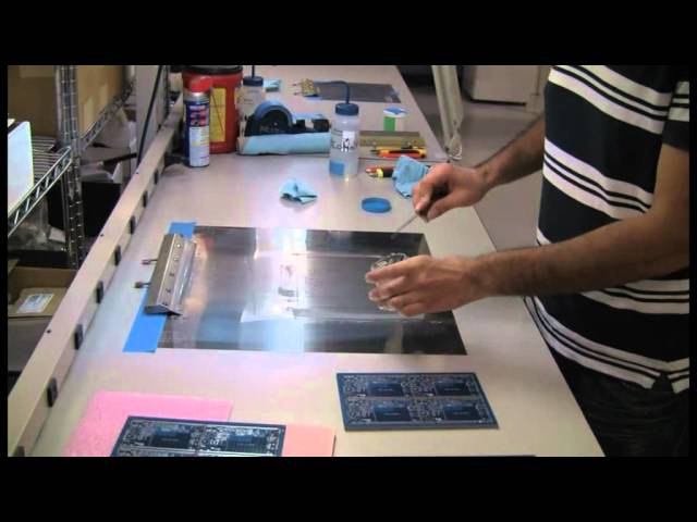
It has been demonstrated in numerous pieces of work that stencil printing, one of the most complex PCB assembly processes, is one of the largest contributors to defects (Revelino et el). This complexity extends to prototype builds where a small number of boards need to be assembled quickly and reliably. Stencil printing is becoming increasingly challenging as packages shrink in size, increase in lead count and require closer lead spacing (finer pitch). Prototype SMT assembly can be further divided between industrial and commercial work and the DIYer, hobbyist or researcher groups. This second group is highly price sensitive when it comes to the materials used for the board assembly as their funds are sourced from personal or research monies as opposed to company funds. This has led to development of a lower cost SMT printing stencil made from plastic film as opposed to the more traditional stainless steel stencil used by industrial and commercial users.This study compares the performance of these two traditional materials and their respective impact on solder paste printing including efficiency and print quality.
Technical Library | 2019-05-29 23:10:30.0
There are times when a PCB prototype needs to be built quickly to test out a design. In such cases where it is known early on that there will be multiple iterations or that a "one and done" assembly will be made that there will be some SMT assemblers who choose to hand print solder paste onto the board using a "frameless" stencil. In such cases where hand printing is used, the consistency of the printing technique has typically been in question. Furthermore, the effectiveness of both the nanocoatings as well as the higher end stainless steel materials, which have been heretofore studied in controlled printing environments, will be evaluated for their impact on the hand printing process.The purpose of the study was to determine the effectiveness of select nanocoating materials as well as certain high end stainless steel stencil materials as they relate to the manual SMT printing process. A variety of nanocoatings were applied to SMT metal stencils and solder paste volume measurements were taken to compare the effectiveness.
Events Calendar | Mon Jul 10 18:30:00 UTC 2023 - Mon Jul 10 18:30:00 UTC 2023 | Oshkosh, Wisconsin USA
Wisconsin Chapter In-Person Event: PCB Workshop and PCB Plant Tour
Events Calendar | Tue Sep 10 18:30:00 UTC 2024 - Tue Sep 10 18:30:00 UTC 2024 | Oshkosh, Wisconsin USA
Wisconsin Chapter In-Person Event: PCB Workshop and PCB Plant Tour
Career Center | San Jose, CA, California USA | Engineering,Production,Research and Development
Senior PCB Designer: Want to be part of an exciting pre-IPO enterprise B2B company working on the cutting edge of internet-of-things, artificial intelligence & agents, blockchain, and manufacturing technology? This well-funded venture-backed co
Career Center | Marietta, Georgia USA | Engineering,Production
Currently seeking a senior pcb designer with Veribest cad experience. Knowledge of RF circuit design parameters, high density, multi-layer, and double sided. Analog/digital smd circuit board strongly desired. Designer will be responsible for pcb boar
Career Center | , | Engineering
PCB Design Engineer using ZUKEN PWS CR5000 & Mentor Graphics CAD from Single-sided PCB board to a Multilayer PCB boards like Mother Board, Notebook, Pheriperal Cards & all Electronics PCB board, from Analog to High Speed Digital Design with the task
Career Center | San Pedro, Laguna Philippines | 2001-02-06 07:34:16.0
1998�present Japan-Philippine Nameplates Inc. Lot 9 Block 13 CEPZ, Rosario, Cavite PCB Design Engineer Designed multi-layer boards. Designed PC Boards for CANON, NEC, EPSON, SONY, FUJITSU, MITSUBISHI, ROHM, NISSEI ELECTRONICS, etc. 1998�1999 PCB Des
SMTnet Express, November 27, 2013, Subscribers: 26387, Members: Companies: 13501, Users: 35461 Improving Density in Microwave Multilayer Printed Circuit Boards for Space Applications by Olivier Vendier, Jean-Louis Cazaux, Jean-Luc Lortal; Thales
SMTnet Express, December 27, 2019, Subscribers: 33,251, Companies: 10,949, Users: 25,451 A Life Prediction Model of Multilayered PTH Based on Fatigue Mechanism Credits: Beihang University PTH plays a critical role in PCB reliability. Thermal
| http://etasmt.com/te_news_industry/2021-10-12/26763.chtml
. Why Is Circuit Board Prototyping Important? Although it may seem that you could generate maximum efficiency by skipping the prototyping step, there are many reasons why this stage is integral to the PCB production process
PCB Libraries, Inc. | https://www.pcblibraries.com/forum/topic3020&OB=ASC.html
. Multi-Board Systems Design Replace inefficient paper and manual processes with an automated, fully integrated, collaborative workflow PCB Simulation Maximize the benefits of PCB virtual prototyping