Utilise Gold contains an international business directory of suppliers of precious metal materials used in the electronics industry, including contacts, plating salts, pastes, solders, bonding wires and evaporation materials.
New Equipment | Rework & Repair Equipment
BEST HotDots™ are designed to simply and cleanly attach jumper wires on a board. HotDots™ are built to survive at high temperature as both the adhesive and the polyimide material are designed to withstand wash and reflow temperatures. HotDots™ are a

New Equipment | Soldering Robots
Laser Hot Bar Soldering Machine with CCD Coaxial Positioning Automatic Vision Product Description The product flows from the track into the welding station. After CCD photography, the tin wire drawing mechanism sends the tin wire to the site to b
Industry News | 2018-10-18 11:08:03.0
Different Techniques for Plating
Industry News | 2018-12-08 03:29:29.0
SMT Dictionary – Surface Mount Technology Acronym and Abbreviation
Technical Library | 2017-09-07 13:56:11.0
As a surface finish for PCBs, Electroless Nickel/Electroless Palladium/Immersion Gold (ENEPIG) was selected over Electroless Nickel/Immersion Gold (ENIG) for CMOS image sensor applications with both surface mount technology (SMT) and gold ball bonding processes in mind based on the research available on-line. Challenges in the wire bonding process on ENEPIG with regards to bondability and other plating related issues are summarized.
Technical Library | 2020-08-27 01:22:45.0
Initially adopted internal specifications for acceptance of printed circuit boards (PCBs) used for wire bonding was that there were no nodules or scratches allowed on the wirebond pads when inspected under 20X magnification. The nodules and scratches were not defined by measurable dimensions and were considered to be unacceptable if there was any sign of a visual blemish on wire-bondable features. Analysis of the yield at a PCB manufacturer monitored monthly for over two years indicated that the target yield could not be achieved, and the main reasons for yield loss were due to nodules and scratches on the wirebonding pads. The PCB manufacturer attempted to eliminate nodules and scratches. First, a light-scrubbing step was added after electroless copper plating to remove any co-deposited fine particles that acted as a seed for nodules at the time of copper plating. Then, the electrolytic copper plating tank was emptied, fully cleaned, and filtered to eliminate the possibility of co-deposited particles in the electroplating process. Both actions greatly reduced the density of the nodules but did not fully eliminate them. Even though there was only one nodule on any wire-bonding pad, the board was still considered a reject. To reduce scratches on wirebonding pads, the PCB manufacturer utilized foam trays after routing the boards so that they did not make direct contact with other boards. This action significantly reduced the scratches on wire-bonding pads, even though some isolated scratches still appeared from time to time, which caused the boards to be rejected. Even with these significant improvements, the target yield remained unachievable. Another approach was then taken to consider if wire bonding could be successfully performed over nodules and scratches and if there was a dimensional threshold where wire bonding could be successful. A gold ball bonding process called either stand-off-stitch bonding (SSB) or ball-stitch-on-ball bonding (BSOB) was used to determine the effects of nodules and scratches on wire bonds. The dimension of nodules, including height, and the size of scratches, including width, were measured before wire bonding. Wire bonding was then performed directly on various sizes of nodules and scratches on the bonding pad, and the evaluation of wire bonds was conducted using wire pull tests before and after reliability testing. Based on the results of the wire-bonding evaluation, the internal specification for nodules and scratches for wirebondable PCBs was modified to allow nodules and scratches with a certain height and a width limitation compared to initially adopted internal specifications of no nodules and no scratches. Such an approach resulted in improved yield at the PCB manufacturer.
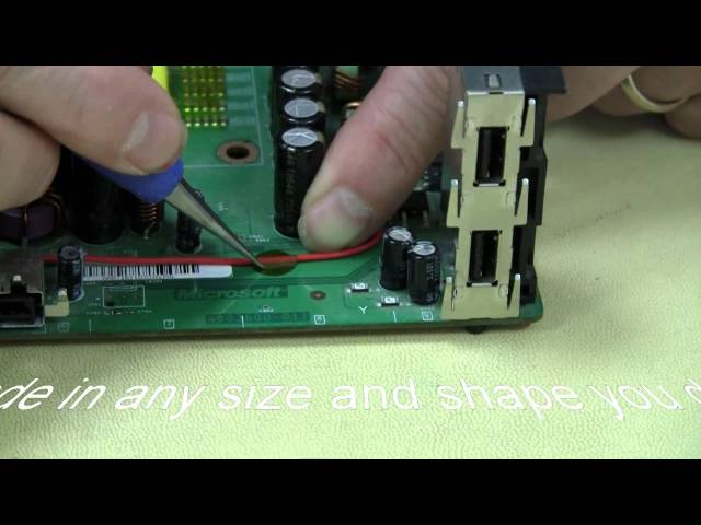
This video demonstrated the use of BEST Inc HotDots(TM) which allow wires to be affixed to the PCB or other surfaces-even when those surfaces go through reflow. There are other similar products out there but none of which can be readily customized no
Events Calendar | Tue Mar 17 18:30:00 UTC 2020 - Tue Mar 17 18:30:00 UTC 2020 | College Park, Maryland USA
CALCE Reliability Science Symposium - Spring 2020
Career Center | Littleton, CO USA | Production
Possess 18 years relevant work experience in manual/Auto bonding on Micro-Electronic & RF to support new product development in R&D Lab in defense & commercial sectors. Have an advanced soldering skill in both Through-Hole/SMT, and J-STD-001 cert
SMTnet Express, September 7, 2017, Subscribers: 30,782, Members: Companies: 10,712, Users: 23,761 Challenges on ENEPIG Finished PCBs: Gold Ball Bonding and Pad Metal Lift Young K. Song and Vanja Bukva; Teledyne DALSA As a surface finish for PCBs
ASYMTEK Products | Nordson Electronics Solutions | https://www.nordson.com/en/divisions/polymer-processing-systems/information/heat-treatments
. The bond of this electroplating is usually not sufficient for screws. The better method, electroless nickel plating, gives an alloy of nickel with up to 15% phosphorous
Surface Mount Technology Association (SMTA) | https://www.smta.org/smtai/best_papers.cfm
: Yoshinori Ejiri, Hitachi Chemical Co., Ltd. " The Wire Bonding Reliability of Electroless Ni/Pd/Au Plating Influence of Electroless Pd Deposition Reaction " View past award winners 2018 1st Place: Richard Coyle, Ph. D


