Industry Directory | Manufacturer
US manufacturer of metallized ceramic substrates & packages; specializing in PCTF (plated copper over thick film) & low cost AgENIG (silver with electroless nickel and immersion gold plating).
Industry Directory | Consultant / Service Provider / Manufacturer
US manufacturer of microelectronic surface mount components including chip resistors, chip attenuators, RF terminations, dividers, splitters, couplers, low pass filters and thermal management devices.
New Equipment | Fabrication Services
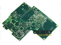
Base Material: FR4 Layer count: 4 layer Board thickness: 1.6mm Copper Thickness:1 oz Surface finish: nickel gold plating Soldermask Colors: Green Size:159.25*182/1up
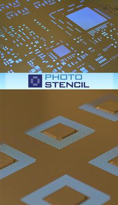
New Equipment | Solder Paste Stencils
NiEX™ electroformed stencils use the same proprietary process as our market leading AMTX™ stencils. The NiEX™ stencil has a higher Knoop Hardness (HK) than our standard AMTX product for those very thin less than .003 applications such as wafer bumpin
Electronics Forum | Thu Oct 30 21:55:13 EDT 2014 | davef
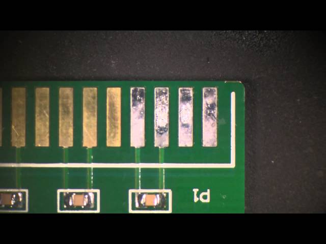
Why soldering issues? I'd guess the nickel is corroded. It is very difficult to solder to oxidized nickel. Your SAC305 would get kicked all the way down the conveyor by nickel oxide. A lack of Ni-Sn-IMC formation will confirm this dewetting . What's
Electronics Forum | Mon Oct 27 20:01:00 EDT 2014 | rangarajd
Hello, We are facing solderability issues on a particular lot of board. THe Nickel thickness measured with an XRF is around 400 U inches. Spec calls out for 130 u inches Nickel and 3 - 5 U inches gold over it. Assuming there is no porosity on the g
Industry News | 2003-05-19 10:06:43.0
The PCB is available with a maximum panel size of 406-by-460mm and a minimum board thickness of 0.8mm.
Industry News | 2003-03-21 08:12:24.0
Tecan reckons it is consistently producing what may be regarded as the most efficient stencils in the world today.
Parts & Supplies | Circuit Board Assembly Products
1) 160*100mm, FR-4 CTI ≥ 600V 2) 8 layer impedance control 3) Copper weight(finished inner/outer): 1 oz 4) LPI Green mask/white silk 5) Min hole 0.19mm, 5/3 track/gap 6) 1.6mm +/-10% thick 7) Immersiong gold over nickel
Parts & Supplies | Circuit Board Assembly Products
1). 1+C+1 HDI, buried/blind L1-L5/L5-L8 vias. 2). FR-4 Material, 1 oz weight. 3). 8 layer, 1.6mm thick. 4). 4/4 mils track and space 5). Min.drill 0.1mm 6). Green solder mask/ white silkscreen 7). Immersion gold over nickel
Technical Library | 2014-08-07 15:13:44.0
Gold embrittlement in SnPb solder is a well-known failure mechanism in electronic assembly. To avoid this issue, prior studies have indicated a maximum gold content of three weight percent. This study attempts to provide similar guidance for Pb-free (SAC305) solder. Standard surface mount devices were assembled with SnPb and SAC305 solder onto printed boards with various thicknesses of gold plating. The gold plating included electroless nickel immersion gold (ENIG) and electrolytic gold of 15, 25, 35, and 50 microinches over nickel. These gold thicknesses resulted in weight percentages between 0.4 to 7.0 weight percent.
Technical Library | 2014-11-06 16:43:24.0
This paper summarizes the results of recent investigations to examine the effect of electroless nickel process variations with respect to Pb-free (Sn-3.0Ag-0.5Cu) solder connections. These investigations included both ENIG and NiPd as surface finishes intended for second level interconnects in BGA applications. Process variations that are suspected to weaken solder joint reliability, including treatment time and pH, were used to achieve differences in nickel layer composition. Immersion gold deposits were also varied, but were directly dependent upon the plated nickel characteristics. In contrast to gold, different electroless palladium thicknesses were independently achieved by treatment time adjustments.
BEST Inc master instructor Norman Mier demonstrates how to replate gold fingers using the BEST gold contact replating kit. In this video he demonstrates how to repair, prepare and replate the finger using a gold replating solution. If you want to lea
Events Calendar | Wed Mar 18 00:00:00 EDT 2020 - Wed Mar 18 00:00:00 EDT 2020 | College Park, Maryland USA
CALCE Reliability Science Symposium - Spring 2020
SMTnet Express, November 6, 2014, Subscribers: 23500, Members: Companies: 14091, Users: 37109 Effect of Process Variations on Solder Joint Reliability for Nickel-based Surface Finishes Hugh Roberts, Sven Lamprecht, Gustavo Ramos, Christian Sebald
ORION Industries | http://orionindustries.com/pdfs/Electrically_conductive_poron.pdf
#180-034 EC-2000 SERIES CONDUCTIVE SILICONES High Performance Foams 171 West St. Charles Road Carol Stream, IL 60188-2081 Tel: 630.784.6200 / Fax: 630.784.6201 www.rogerscorporation.com Technical Data TYPICAL PROPERTIES Test Method Filler Base Polymer Specific Gravity, g/cc Thickness
ASYMTEK Products | Nordson Electronics Solutions | https://www.nordson.com/en/divisions/polymer-processing-systems/information/heat-treatments
. The advantages of electroless over electro nickel are: (1) Uniform in thickness, even in deep recesses; (2) Non-porous; (3) Some ability to obtain higher hardness by baking; and (4) Better adhesion


