Industry News | 2010-09-13 15:36:15.0
IPC — Association Connecting Electronics Industries® has released IPC-1601, Printed Board Handling and Storage Guidelines. The industry's sole standard on the handling, packaging and storage of printed boards, IPC-1601 provides users with guidance on how to protect printed boards from contamination, physical damage, solderability degradation, electrostatic discharge and moisture uptake.
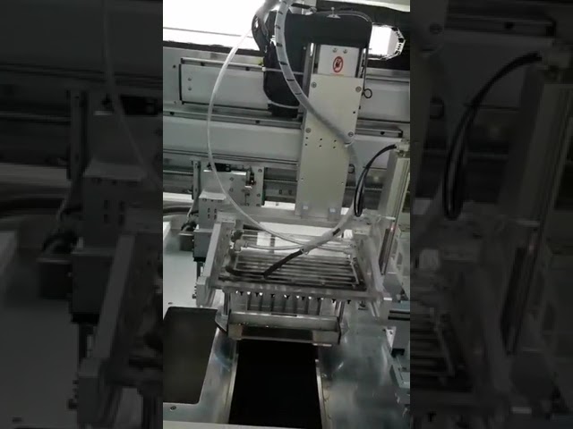
Full Automatic V-cut PCB Depaneler Introduction: This equipment can further improve the quality of depaneling. It can realize V-groove XY two-way automatic cutting, cutting aluminum & FR4 boards without burr, can connect the assembly line to realize
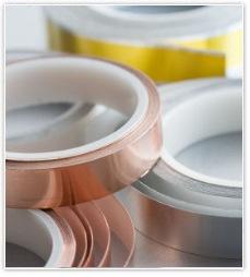
Conductive Foil Tapes Our range of conductive foil tape offers a cost-effective solution to EMC shielding. Tapes are available in both copper and aluminium with a conductive adhesive. The tapes can be used to seal joints on enclosures and for ground
Technical Library | 2018-09-21 10:12:53.0
Moisture accumulates during storage and industry practice recommends specific levels of baking to avoid delamination. This paper will discuss the use of capacitance measurements to follow the absorption and desorption behaviour of moisture. The PCB design used in this work, focused on the issue of baking out moisture trapped between copper planes. The PCB was designed with different densities of plated through holes and drilled holes in external copper planes, with capacitance sensors located on the inner layers. For trapped volumes between copper planes, the distance between holes proved to be critical in affecting the desorption rate. For fully saturated PCBs, the desorption time at elevated temperatures was observed to be in the order of hundreds of hours. Finite difference diffusion modelling was carried out for moisture desorption behaviour for plated through holes and drilled holes in copper planes. A meshed copper plane was also modelled evaluating its effectiveness for assisting moisture removal and decreasing bake times. Results also showed, that in certain circumstances, regions of the PCB under copper planes initially increase in moisture during baking.
With the development of miniaturization of assembly components, the layout area and pattern design area of PCBs have also been continuously reduced, and PCB manufacturers are constantly updating the production process to conform to the development tr
Industry News | 2019-05-16 01:24:13.0
With the development of miniaturization of assembly components, the layout area and pattern design area of PCBs have also been continuously reduced, and PCB manufacturers are constantly updating the production process to conform to the development trend. The application of the resin plugging process has also become more and more extensive, and it has been used in HDI panels.
Industry News | 2016-08-19 05:00:52.0
If you have a process problem, let NPL Defect of the Month Video help you team
500⁰C) Compatible with multiple lamination cycles Standard PCB lamination cycles may be used Excellent for Laser Via formation Excellent CAF resistance Uses standard desmear and plating processes High Modulus: 1100 kpsi Lo
Industry News | 2023-11-13 12:31:47.0
Circuit Technology Center announces it has added the capability to trim and form electronic component packages to customers' exact pre-assembly specifications. They can also propose a trim and lead-form drawing if needed. Dedicated, custom tooling can be fabricated to meet custom package requirements.


