Training Courses | | | IPC-600 Specialist (CIS)
The Certified IPC-600 Specialist (CIS) training targets quality assurance and acceptance of bare printed circuit boards.
Industry News | 2022-11-15 12:33:16.0
SHENMAO America, Inc is pleased to introduce its newest offering: PF735-EP307 Joint Enhanced Solder Paste (JEP). The new low melting point epoxy-based solder material has been developed for extremely fine-pitch or fine pad soldering, especially advanced display assembly.
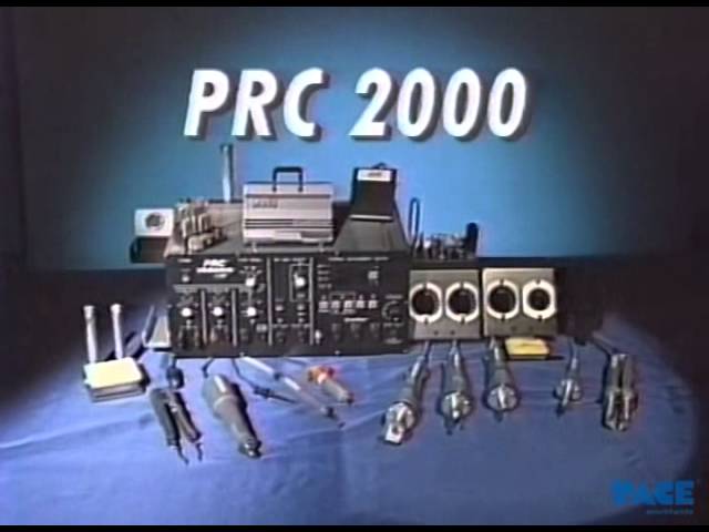
http://paceworldwide.com/products/conductive-rework-systems/prc-2000/prc-2000-pace-repair-center-the-benchtop The PRC 2000 Benchtop Factory is the ultimate rework center. The PRC 2000 can tackle just about any Thru-Hole, SMT application and is well
Industry Directory | Association / Non-Profit
The largest society dedicated to the advancement and growth of microelectronics and electronics packaging technologies. IMAPS produces numerous workshops, conferences, professional development courses, and exhibitions.
Industry Directory | Manufacturer
An innovative thermal management company that is dedicated to address the thermal challenges that the electronics industry is facing.
Industry Directory | Association / Non-Profit
An independent body of ESD experts with the mission to review the ESD robustness requirements of modern IC products for allowing safe handling and mounting
Specifically engineered for water resistance on printed circuit board protection and LED component protection in membrane switches. Surface Resistivity: 3.8 x 10¹⁴ ω/■ Insulation resistance of cured films of UV-3010 at 100°C and 95% relative h
Technical Library | 2015-12-02 18:32:50.0
(Thermal Compression with Non-Conductive Paste Underfill) Method.The companies writing this paper have jointly developed Copper (Cu) Pillar micro-bump and TCNCP(Thermal Compression with Non-Conductive Paste) technology over the last two+ years. The Cu Pillar micro-bump and TCNCP is one of the platform technologies, which is essentially required for 2.5D/3D chip stacking as well as cost effective SFF (small form factor) package enablement.Although the baseline packaging process methodology for a normal pad pitch (i.e. inline 50μm) within smaller chip size (i.e. 100 mm2) has been established and are in use for HVM production, there are several challenges to be addressed for further development for commercialization of finer bump pitch with larger die (i.e. ≤50μm tri-tier bond pad with the die larger than 400mm2).This paper will address the key challenges of each field, such as the Cu trace design on a substrate for robust micro-joint reliability, TCNCP technology, and substrate technology (i.e. structure, surface finish). Technical recommendations based on the lessons learned from a series of process experimentation will be provided, as well. Finally, this technology has been used for the successful launching of the company FPGA products with SFF packaging technology.
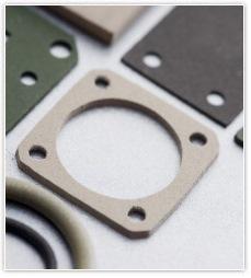
Our range of connector gaskets includes precision diecut gaskets made from a large selection of materials, both conductive and non-conductive. The DC Series comprises waveguide and connector gaskets to MIL-C-81511, MIL-C-5015, MIL-C-38999 and MIL-C-
Industry News | 2021-03-02 14:45:26.0
SHENMAO America, Inc. is pleased to introduce its newJoint Enhanced Solder Paste (JEP) PF606-EP305 and Solder Joint Encapsulation Material (SJEM) Flux SMEF-Z52. The new epoxy-based solder materials for very fine pad size (70 μm) soldering, especially for advanced display packaging and assembly.


.png)