SMt BGA Rework and Repair Equipment including Split Vision processes and lead free soldered product rework application. Thru-Hole Desoldering and Plating Equipment.
Industry Directory | Manufacturer
1-20 layers PCB manufacturer, focusing on metal core pcb, multi-layer PCB, fast PCB and middle-small batch PCB. Min. circuit width & spacing: 3mil. UL, ISO9001, ROHS,ISO14001 certified.
Training Courses | | | IPC-600 Specialist (CIS)
The Certified IPC-600 Specialist (CIS) training targets quality assurance and acceptance of bare printed circuit boards.
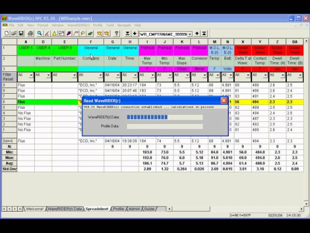
The following video guides the user through a typical data collection process. These steps may vary depending on the process your company uses. Categories: WaveRIDER, WaveRIDER SPC (v5.2x)
Industry Directory | Manufacturer / Other
Founded in 1968, EPE is a third generation, veteran-owned, ITAR registered provider of complex electronic contract manufacturing services including printed circuit board assembly, electromechanical assembly, and system assembly
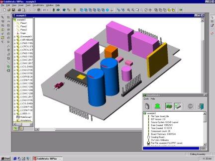
CircuitWorks is a fully integrated data interface between SolidWorks and PCB Design systems. Running totally inside SolidWorks, CircuitWorks will read an industry-standard IDF file, and produce a SolidWorks 3D Assembly of the PCB board fully populat
New Equipment | Wave Soldering
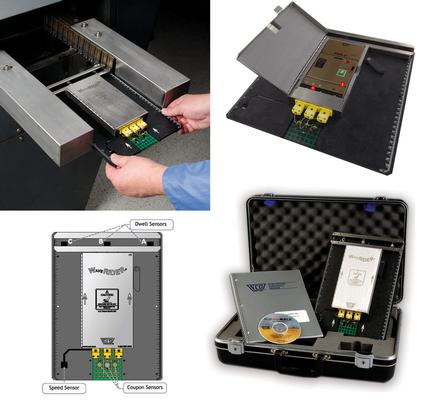
The only portable wave soldering machine optimizers with statistical process control (SPC) The wave soldering process is one of the most challenging procedures to set up. The ECD WaveRIDER® NL 2 greatly simplifies wave solder set up and ensures perf
Technical Library | 2021-06-21 19:34:02.0
In this era of electronics miniaturization, high yield and low-cost integrated circuit (IC) substrates play a crucial role by providing a reliable method of high density interconnection of chip to board. In order to maximize substrate real-estate, the distance between Cu traces also known as line and space (L/S) should be minimized. Typical PCB technology consists of L/S larger than 40 µ whereas more advanced wafer level technology currently sits at or around 2 µm L/S. In the past decade, the chip size has decreased significantly along with the L/S on the substrate. The decreasing chip scales and smaller L/S distances has created unique challenges for both printed circuit board (PCB) industry and the semiconductor industry. Fan-out panel-level packaging (FOPLP) is a new manufacturing technology that seeks to bring the PCB world and IC/semiconductor world even closer. While FOPLP is still an emerging technology, the amount of high-volume production in this market space provide a financial incentive to develop innovative solutions in order to enable its ramp up. The most important performance aspect of the fine line plating in this market space is plating uniformity or planarity. Plating uniformity, trace/via top planarity, which measures how flat the top of the traces and vias are a few major features. This is especially important in multilayer processing, as nonuniformity on a lower layer can be transferred to successive layers, disrupting the device design with catastrophic consequences such as short circuits. Additionally, a non-planar surface could also result in signal transmission loss by distortion of the connecting points, like vias and traces. Therefore, plating solutions that provide a uniform, planar profile without any special post treatment are quite desirable.
Industry News | 2019-11-05 22:22:32.0
1. The definition of Sideplating Sideplating is actually the metalization of the board edge in PCB filed. Edge plating、Border plated、plated contour、side metal, these words can be used too to describe same function. 2. Sideplating Process Drilling - Milling plated Slots - Cleaning - Copper sink 3. Pictures to show the finished board’s sideplating
Training Courses | | | PCB Assembly Courses
The PCB assembly courses provide knowledge of different processes and equipment used in TH and SMT assembly of printed circuit boards.


