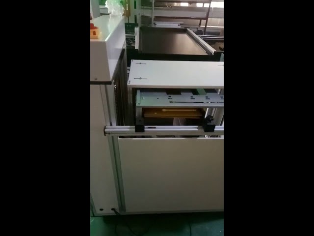
Jwide PCB magzine loader is used to load PCB to production. different models for different PCB sizes User friendly touch screen Single or multi magzines optional Welcome details: sales@jwide-smt.com
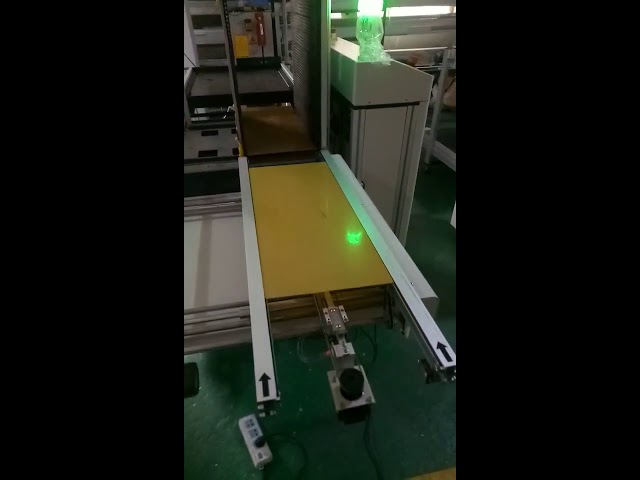
Automatic PCB magazine unloaders is used to load or unload PCB before or after production. Single or dual magzine for option specially designed for 0.6M LED strip Welcome details: sales@jwide-smt.com
Jwide PCB magzine loader is used to load PCB to production. different models for different PCB sizes User friendly touch screen Single or multi magzines optional Welcome details: sales@jwide-smt.com
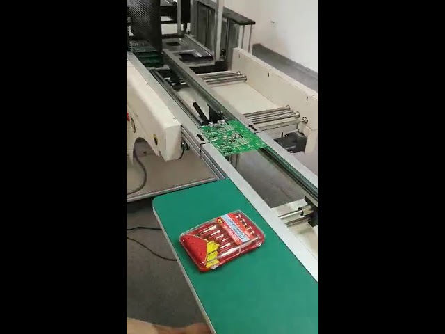
Jwide PCB unloader is used to unload PCB after soldering process
2 containers of 500g at the same time container diameter:60~66mm for details: www.jwide-smt.com or Mail: sales@jwide-smt.com

2 containers of 500g at the same time container diameter:60~66mm for details: www.jwide-smt.com or Mail: sales@jwide-smt.com
Industry News | 2017-05-01 14:53:34.0
ITW EAE’s Vitronics Soltec earned two coveted VA Excellent Awards from the SMT China Vision Awards at the recent NEPCON China exposition and conference in Shanghai. The CATHOX™ Catalytic Thermal Oxidizer was recognized in the Reflow Soldering category and the ZEVAm took the prize in the Selective Soldering category.
Industry News | 2020-11-24 00:27:11.0
Research on non-precious metal catalysts. Research progress of non-precious metal catalysts for proton exchange membrane fuel cells
Technical Library | 1999-05-07 08:50:40.0
To enable transistor scaling into the 21st century, new solutions such as high dielectric constaConventional scaling of gate oxide thickness, source/drain extension (SDE), junction depths, and gate lengths have enabled MOS gate dimensions to be reduced from 10mm in the 1970’s to a present day size of 0.1mm. To enable transistor scaling into the 21st century, new solutions such as high dielectric constant materials for gate insulation and shallow, ultra low resistivity junctions need to be developed. In this paper, for the first time, key scaling limits are quantified for MOS transistorsnt materials for gate insulation and shallow, ultra low resistivity junctions need to be developed.
Technical Library | 2012-12-14 14:28:20.0
This paper examines the potential failure mechanisms that can damage modern lowvoltage CMOS devices and their relationship to electrical testing. Failure mechanisms such as electrostatic discharge (ESD), CMOS latch-up, and transistor gate oxide degradation can occur as a result of electrical over-voltage stress (EOS). In this paper, EOS due to electrical testing is examined and an experiment is conducted using pulsed voltage waveforms corresponding to conditions encountered during in-circuit electrical testing. Experimental results indicate a correlation between amplitude and duration of the pulse waveform and device degradation due to one or more of the failure mechanisms.


