New Equipment | Board Handling - Storage
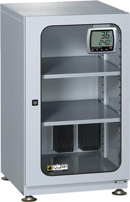
Effective moisture damage solution that improves yields. http://eurekadrytech.com/fast-super-dryer/tus-101 Capacity: 93 Liters Humidity Range: 10%-50% Recovery Time: Recovers to ≤ 20% RH within 2 hours after accessing door for 30 seconds or les
Technical Library | 2013-12-27 10:39:21.0
The head-in-pillow defect has become a relatively common failure mode in the industry since the implementation of Pb-free technologies, generating much concern. A head-in-pillow defect is the incomplete wetting of the entire solder joint of a Ball-Grid Array (BGA), Chip-Scale Package (CSP), or even a Package-On-Package (PoP) and is characterized as a process anomaly, where the solder paste and BGA ball both reflow but do not coalesce. When looking at a cross-section, it actually looks like a head has pressed into a soft pillow. There are two main sources of head-in-pillow defects: poor wetting and PWB or package warpage. Poor wetting can result from a variety of sources, such as solder ball oxidation, an inappropriate thermal reflow profile or poor fluxing action. This paper addresses the three sources or contributing issues (supply, process & material) of the head-in-pillow defects. It will thoroughly review these three issues and how they relate to result in head-in pillow defects. In addition, a head-in-pillow elimination plan will be presented with real life examples will be to illustrate these head-in-pillow solutions.
Technical Library | 2017-03-02 18:13:05.0
The need for more energy-efficient solid-state switches beyond complementary metal-oxide-semiconductor (CMOS) transistors has become a major concern as the power consumption of electronic integrated circuits (ICs) steadily increases with technology scaling. Nano-Electro-Mechanical (NEM) relays control current flow by nanometer-scale motion to make or break physical contact between electrodes, and offer advantages over transistors for low-power digital logic applications: virtually zero leakage current for negligible static power consumption; the ability to operate with very small voltage signals for low dynamic power consumption; and robustness against harsh environments such as extreme temperatures. Therefore, NEM logic switches (relays) have been investigated by several research groups during the past decade. Circuit simulations calibrated to experimental data indicate that scaled relay technology can overcome the energy-efficiency limit of CMOS technology. This paper reviews recent progress toward this goal, providing an overview of the different relay designs and experimental results achieved by various research groups, as well as of relay-based IC design principles. Remaining challenges for realizing the promise of nano-mechanical computing, and ongoing efforts to address these, are discussed.
Technical Library | 2019-02-20 16:35:24.0
The High Density Packaging (HDP) User Group has completed a project evaluating the high frequency loss impacts of a variety of imaged core surface treatments (bond enhancement treatments, including chemical bonding and newer low etch alternative oxides) applied just prior to press lamination. Initial high frequency Dk/Df electrical test results did not show a strong correlation with any of the methods utilized within this project to measured surface roughness. The more significant factor affecting the measured loss is the choice of pre-lamination surface treatment. Most of the new chemical treatment systems outperform the older existing systems which depend upon surface roughness techniques to promote adhesion.
Technical Library | 2019-07-02 23:02:05.0
The introduction of lead-free solders resulted in a selection of different chemistries for solder pastes. The higher melting points of lead-free alloys required thermal heat resistant rosin systems and activators that are active at elevated temperatures. As a result, more frequent maintenance of the filtration systems is required and machine downtime is increased.Last year a different method of cleaning reflow ovens was introduced. Instead of cooling down the process gasses to condensate the residues, a catalyst was used to maintain the clean oven. Catalytic thermal oxidation of residues in the nitrogen atmosphere resulted in cleaner heating zones. The residues were transformed into carbon dioxide. This remaining small amount of char was collected in the catalyst. In air ovens the catalyst was not seen as a beneficial option because the air extracted out of the oven was immediately exhausted into the environment. When a catalyst is used in an air environment there is not only the carbon dioxide residues, but also water. When a catalyst is used in an air reflow oven the question is where the water is going to. Will it condensate in the process part of the oven or is the gas temperature high enough to keep it out of the process area? A major benefit of using a catalyst to clean the air before it is exhausted into the environment is that the air pollution is reduced dramatically. This will make environmental engineers happy and result in less pollution of our nature. Apart from this, the exhaust tubes remain clean which reduces the maintenance of air ovens.This paper will give more detailed information of catalyst systems during development and performance in production lines.
Technical Library | 2019-10-29 02:55:33.0
For every 10 ℃ increase in temperature, the reaction rate is twice to three times. This means that for every 10 ℃ increase in temperature, the life span of the product will be halved, and when the temperature rises by 20 ℃, the life span of the product will be reduced to 1/4. High temperature will lead to aging, oxidation, evaporation, physical deformation and so on. Low temperature will lead to embrittlement, ice formation, viscosity and solidification degree, loss of mechanical strength, physical shrinkage and so on. When the product is shipped, stored and operated in the environment, it will be endangered. In addition, each product has regulatory and certification requirements, and it is important to evaluate reliability and durability before it is put on the market. In general, according to the IEC60068 test standard, it requires the volume of the laboratory to be at least five times the total volume of the sample under test. Haida constant temperature and humidity box can help you meet this demand. So with the fast developmement of manufacturing industry,test becomes a necessity to see wether the product is able to meet regulated standards in R&D satge,Climatest Symor specializes in handling temperature and humidity,we supply environmental test chamber to China State-owned Research Institutes and laboratories,and obtain excellent reputation from international cllients,our company put much efforts on chamber R&D ,striving to supply best-quality climate simulation equipment and after-sale service. For details,pls visit our official website www.climatechambers.com
Technical Library | 2020-10-14 14:33:36.0
Epoxy based adhesives are prevalent interface materials for all levels of electronic packaging. One reason for their widespread success is their ability to accept fillers. Fillers allow the adhesive formulator to tailor the electrical and thermal properties of a given epoxy. Silver flake allow the adhesive to be both electrically conductive and thermally conductive. For potting applications, heat sinking, and general encapsulation where high electrical isolation is required, aluminum oxide has been the filler of choice. Today, advanced Boron Nitride filled epoxies challenge alternative thermal interface materials like silicones, greases, tapes, or pads. The paper discusses key attributes for designing and formulating advanced thermally conductive epoxies. Comparisons to other common fillers used in packaging are made. The filler size, shape and distribution, as well as concentration in the resin, will determine the adhesive viscosity and rheology. Correlation's between Thermal Resistance calculations and adhesive viscosity are made. Examples are shown that determination of thermal conductivity values in "bulk" form, do not translate into actual package thermal resistance. Four commercially available thermally conductive adhesives were obtained for the study. Adhesives were screened by shear strength measurements, Thermal Cycling ( -55 °C to 125 °C ) Resistance, and damp heat ( 85 °C / 85 %RH ) resistance. The results indicate that low modulus Boron Nitride filled epoxies are superior in formulation and design. Careful selection of stress relief agents, filler morphology, and concentration levels are critical choices the skilled formulator must make. The advantages and limitations of each are discussed and demonstrated.
Technical Library | 2021-11-03 16:52:47.0
This paper proposes the integration of pulsed photonic sintering into multi-material additive manufacturing processes in order to produce multifunctional components that would be nearly impossible to produce any other way. Pulsed photonic curing uses high power Xenon flash lamps to thermally fuse printed nanomaterials such as conductive metal inks. To determine the feasibility of the proposed integration, three different polymer additive manufacturing materials were exposed to typical flash curing conditions using a Novacentrix Pulseforge 3300 system. FTIR analysis revealed virtually no change in the polymer substrates, thus indicating that the curing energy did not damage the polymer. Next, copper traces were printed on the same substrate, dried, and photonically cured to establish the feasibility of thermally fusing copper metal on the polymer additive manufacturing substrates. Although drying defects were observed, electrical resistivity values ranging from 0.081 to 0.103 Ω/sq. indicated that high temperature and easily oxidized metals can be successfully printed and cured on several commonly used polymer additive manufacturing materials. These results indicate that pulsed photonic curing holds tremendous promise as an enabling technology for next generation multimaterial additive manufacturing processes.
Industry News | 2001-12-03 07:45:41.0
Motorola to Preview Next-Generation 0.10 micron CMOS Technology and New Gate Dielectric Material at World's Leading Semiconductor Device Conference
Industry News | 2017-12-19 19:54:07.0
Indium Corporation will feature Indium11.8HF-SPR Solder Paste – a new air and nitrogen reflow, no-clean, Pb-free solder paste designed to meet the fine feature printing requirements of mobile manufacturers – at IPC APEX Expo 2018, Feb. 24-March 1 in San Diego, Calif.


