
New Equipment | Solder Materials
For high density and advanced package technology, We provide new Solder Paste for PoP applications. Package on Package Solder Paste has better wettability, solderability and low void than others.
New Equipment | Industrial Automation
About SIEMENS Its electronic and electrical products are global industry pioneers and are active in energy, medical, industrial, infrastructure and urban business fields. Skype : dddemi33 QQ :2851195473 Sales Manager : Tiffany Guan Email me
Industry News | 2015-08-03 17:18:00.0
Join BEST and 50+ engineers on October 1 in this technical symposium featuring excellent speakers and topics
Industry News | 2015-08-05 10:32:21.0
SMT micro electronics assembly and rework symposium has been scheduled for 2015 for October 1, 2015. Learn/Re-learn how to perform a design of experiments, learn rework tips from Paul Wood and "lessons learned" from Chrys Shea.
Technical Library | 2012-12-17 22:05:22.0
Package on Package (PoP) has become a relatively common component being used in mobile electronics as it allows for saving space in the board layout due to the 3D package layout. To insure device reliability through drop tests and thermal cycling as well as for protecting proprietary programming of the device either one or both interconnect layers are typically underfilled. When underfill is applied to a PoP, or any component for that matter, there is a requirement that the board layout is such that there is room for an underfill reservoir so that the underfill material does not come in contact with surrounding components. The preferred method to dispensing the underfill material is through a jetting process that minimizes the wet out area of the fluid reservoir compared to traditional needle dispensing. To further minimize the wet out area multiple passes are used so that the material required to underfill the component is not dispensed at once requiring a greater wet out area. Dispensing the underfill material in multiple passes is an effective way to reduce the wet out area and decrease the distance that surrounding components can be placed, however, this comes with a process compromise of additional processing time in the underfill dispenser. The purpose of this paper is to provide insight to the inverse relationship that exists between the wet out area of the underfill reservoir and the production time for the underfill process.
Technical Library | 2010-03-23 11:50:22.0
This document discuss how to design SMT stencil base on IPC-7525. Introduction: PCBA (Printed Circuit Board Assembly) is a segment of printed circuit board technology. This segment of printed circuit board industry is concentrated in assemble all the pieces of electronic industry to one piece before output them to market. This segment covers: interconnection technology, package design technology, system integration technology, board and system test technology

Flux spray coating on a PCB with uniformal thickness down to 5 microns, with clear edge definition and minimal overspray. Can coat large or shoot dots with the same jet.
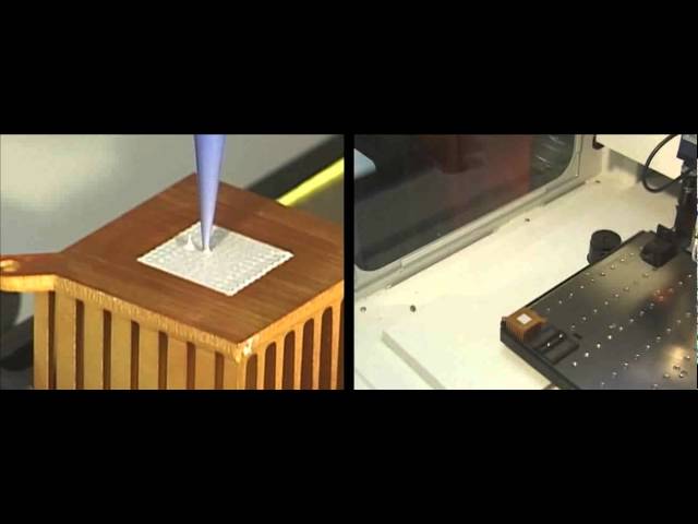
Precise lines are dispensed to fill an area on a heat sink. At the end of this video, you can see a demo of placing a glass slide on top of the dispensed material to see uniformity of the area. http://www.nordsonasymtek.com
Events Calendar | Tue Aug 18 18:30:00 UTC 2020 - Tue Aug 18 18:30:00 UTC 2020 | ,
DfR - Design for Rinse-Ability: Effect of SMT Component Package Design on Cleaning Effectiveness
Events Calendar | Sun Mar 01 18:30:00 UTC 2020 - Wed Mar 04 18:30:00 UTC 2020 | Fountain Hills, Arizona USA
16th International Conference and Exhibition on DEVICE PACKAGING
International Microelectronics Assembly and Packaging Society (IMAPS)
SMTnet Express, December 16, 2021, Subscribers: 26,148, Companies: 11,476, Users: 26,983 Assembly and Rework of Lead Free Package on Package Technology Miniaturization continues to be a driving force in both integrated circuit
SMTnet Express, July 21, 2022, Subscribers: 25,294, Companies: 11,589, Users: 27,357 █ Electronics Manufacturing Technical Articles Assembly and Rework of Lead Free Package on Package Technology Miniaturization continues to be a driving
GPD Global | https://www.gpd-global.com/pdf/lead-former/CF9-Doc-Package-901-1-01.pdf
Instructions I M P O R T A N T Read this manual before turning the power on. Failure to follow the instructions in this manual could result in damage to the machine and/or dies. Uneven forming of the component leads and/or machine failure could result
PCB Libraries, Inc. | https://www.pcblibraries.com/forum/topic1208&OB=ASC.html
SC-82AB Package - PCB Libraries Forum Forum Home > Libraries > Footprints / Land Patterns New Posts FAQ Search Events Register Login SC-82AB Package


