This module adds creation of thick-film, thin-film, laminate and ceramic MCMs. Dies are easily captured from any type of data (faxed, standard data files or GDSII). Bonding pads made with any number of rows, straight or curved, fanouts using equal
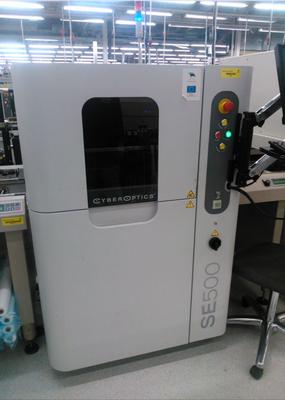
Used SMT Equipment | SPI / Solder Paste Inspection
All the machines have been maintained by the manufacturer or the official distributor in accordance with required maintenance schedule. ASK QUOTATION! Dimensions Unit Height 139 cm (55 in.) excluding signal-light pole and leveling feet Unit Wi
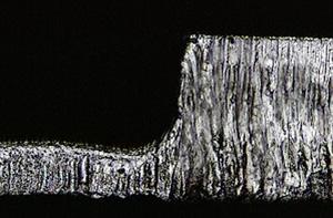
New Equipment | Solder Paste Stencils
Through the increase of mixed technologies, stepped stencils have gained importance to the electronic assembly manufacturer. If the solder paste quantity can no longer be adequately regulated by adjusting Step/Relief Stencil Picture the pad sizes, st
Technical Library | 2015-12-31 15:19:28.0
Today's consumer electronic product are characterized by miniatuization, portability and light weight with high performance, especially for 3G mobile products. In the future more fine pitch CSPs (0.4mm) component will be required. However, the product reliability has been a big challenge with the fine pitch CSP. Firstly, the fine pitch CSPs are with smaller solder balls of 0.25mm diameter or even smaller. The small solder ball and pad size do weaken the solder connection and the adhesion of the pad and substrate, thus the pad will peel off easily from the PCB substrate. In addition, miniature solder joint reduce the strength during mechanical vibration, thermal shock, fatigue failure, etc. Secondly, applying sufficient solder paste evenly on the small pad of the CSP is difficult because stencil opening is only 0.25mm or less. This issue can be solved using the high end type of stencil such as Electroforming which will increase the cost.

New Equipment | Assembly Services
Quick turn Prototype PCBs from 24 hour turnaround to high volume printed circuit board production from our domestic plant in USA and/or China facilities. Our Modern 38,000 sq. ft. manufacturing plant with multi-million dollar investment with latest e


See what some of our customers have to say about the complete PCB design environment offered by PADS 9.0. This next generation in PCB Design tool combines an intuitive, flexible design environment with integrated, scalable technology. Giving engine
Industry News | 2019-11-05 22:08:21.0
Via in pad is the design practice of placing a via in the copper landing pad of a component. Compared to standard PCB via routing, via in pad allows a design to use smaller component pitch sizes and further reduce the PCBs overall size. With component manufactures pushing smaller parts every year and the demand from consumers for smaller devices, the usage of via in pad practices by hardware engineers have become more commonplace. In this article, we will discuss the differences between via in pad and traditional vias, when should you use via in pad, and how to design for it.
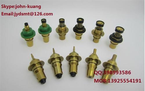
Parts & Supplies | Other Equipment
JUKI SMT NOZZLE FOR 700 SERIES SPECS: JUKI 700 Series SMT NOZZLE Part Number (OEM) Description E3501 - 721 - 0A0 101 ASSEMBLY ø 1.0/ ø 0.4 E3502 - 721 - 0A0 102 ASSEMBLY ø 1.5/ ø 1.0 E3503 - 721 - 0A0 103 ASSEMBLY ø 3.0/ ø 1.7 E3504 - 721 -
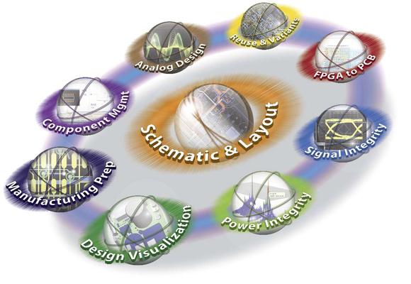
A complete, but lower-cost PCB design solution for smaller organizations or individuals PADS®, Mentor Graphics’ world-leading desktop PCB design tool, enables you to develop PCBs within a highly productive, scalable, and easy-to-use environment.


