Industry News | 2012-06-26 14:16:01.0
Count On Tools Inc.introduces the new ezLOAD XL PCB Support System.

1200MM/1500MM Online SPI , Big Size Solder Paste Inspection Machine mail: sales@smtlinemachine.com whatapp/wechat:+8613537875415 Specification: 技术参数/Parameters 技术平台/Technology Platform super big size platform 适用
Inline 3D SPI, Standard Automatic solder paste inspection system As one of the strongest SMT 3D SPI Manufacuturer in China, we provide you all the different models of online solder paste inspection machine,we have variety of size and models of the

Parts & Supplies | Chipshooters / Chip Mounters
> JUKI ESL13000000 VACUUM PAD 15 JUKI ESL13000100 PHOTO MICRO SENSOR A JUKI ESL13001000 TUBE union (KL700) JUKI ESL130011A0 CONVEYOR MOTOR (KZ500) JUKI ESL13002000 CLAMP LEVER JUKI ESL13003000 T TYPE NUT JUKI ESL130031A0 OPERATION PANEL (KL700) JUKI
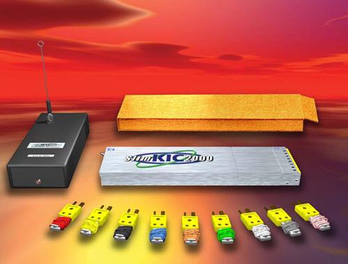
Click here to view the SlimKIC 2000 datasheet Profiling So Easy, Anyone Can Do It By automating the complex task of process set up the SlimKIC® 2000™ makes profiling so easy that any operator can quickly achieve the optimal process. Simply select fro

Click here to view the SlimKIC 2000 datasheet Profiling So Easy, Anyone Can Do It By automating the complex task of process set up the SlimKIC® 2000™ makes profiling so easy that any operator can quickly achieve the optimal process. Simply select fro
Users can now spend under $800.00 USD and receive a feature-filled DMM with 11 measurement and 8 math functions. Other important considerations are its noise immunity, USB with 2000 measurements and transfers/sec 10-channel scan option, temperature m
Technical Library | 2020-08-27 01:22:45.0
Initially adopted internal specifications for acceptance of printed circuit boards (PCBs) used for wire bonding was that there were no nodules or scratches allowed on the wirebond pads when inspected under 20X magnification. The nodules and scratches were not defined by measurable dimensions and were considered to be unacceptable if there was any sign of a visual blemish on wire-bondable features. Analysis of the yield at a PCB manufacturer monitored monthly for over two years indicated that the target yield could not be achieved, and the main reasons for yield loss were due to nodules and scratches on the wirebonding pads. The PCB manufacturer attempted to eliminate nodules and scratches. First, a light-scrubbing step was added after electroless copper plating to remove any co-deposited fine particles that acted as a seed for nodules at the time of copper plating. Then, the electrolytic copper plating tank was emptied, fully cleaned, and filtered to eliminate the possibility of co-deposited particles in the electroplating process. Both actions greatly reduced the density of the nodules but did not fully eliminate them. Even though there was only one nodule on any wire-bonding pad, the board was still considered a reject. To reduce scratches on wirebonding pads, the PCB manufacturer utilized foam trays after routing the boards so that they did not make direct contact with other boards. This action significantly reduced the scratches on wire-bonding pads, even though some isolated scratches still appeared from time to time, which caused the boards to be rejected. Even with these significant improvements, the target yield remained unachievable. Another approach was then taken to consider if wire bonding could be successfully performed over nodules and scratches and if there was a dimensional threshold where wire bonding could be successful. A gold ball bonding process called either stand-off-stitch bonding (SSB) or ball-stitch-on-ball bonding (BSOB) was used to determine the effects of nodules and scratches on wire bonds. The dimension of nodules, including height, and the size of scratches, including width, were measured before wire bonding. Wire bonding was then performed directly on various sizes of nodules and scratches on the bonding pad, and the evaluation of wire bonds was conducted using wire pull tests before and after reliability testing. Based on the results of the wire-bonding evaluation, the internal specification for nodules and scratches for wirebondable PCBs was modified to allow nodules and scratches with a certain height and a width limitation compared to initially adopted internal specifications of no nodules and no scratches. Such an approach resulted in improved yield at the PCB manufacturer.
Industry News | 2018-10-18 08:34:52.0
How to Prevent Solder Bridging in 3528 PLCC6 RGB LEDs?


