Industry Directory | Manufacturer
Depanelizer Equipment and Tools For Electronic Assembly. PCB Racks and Trays. Wire Crimp Press and Tooling.

Industry Directory | Manufacturer
A leader in automated fluid dispensing, jetting, and conformal coating. Products include stand-alone dispensing workstations and fully automated, in-line conveyorized systems with advanced process controls.

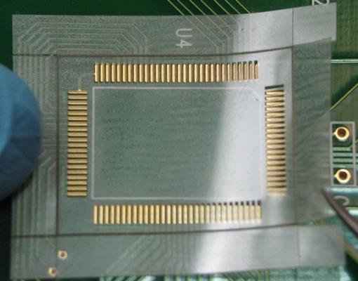
If you have boards requiring high tolerance mechanical dimension or odd shapes that traditional depaneling methods cannot handle. BEST Inc. provides laser depaneling services for printed circuit board manufacturers as well as EMS and OEMs. BEST’s nu
New Equipment | Solder Paste Stencils
Sometimes there are products that come along and you think to yourself-Wow! The StikNPeel™ rework stencil is one of those products. It simplifies the rework of site locations by placing a highly flexible, removable, adhesive-backed stencil on to a ci
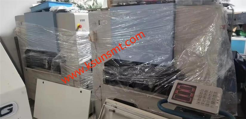
Used SMT Equipment | Chipshooters / Chip Mounters
Refurbished YV180XG Pick and Place Machine Panel size L Type: Max L380 x W330 mm ∼ Min L50 x W50 mm Panel thick 0.4 ~ 3.0 mm Mounting ±0.05 mm (0.01mm control) Mounting angle ±180° (0.01° control) Mounting speed 0.095 se
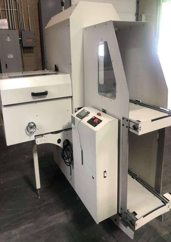
Used SMT Equipment | Conveyors
Conveyor Technologies MAG-ALL-R Loader/Unloader Date of Manufacture: 2010 Details: Vertical FIFO/LIFO/Pass Through/Magazine Loader/Unloader Removable Magazine (Magazines Sold Separately) Mechanical Pusher Used to Load and Unload PCBs Adjust PCB
Industry News | 2011-11-20 13:36:13.0
GPD Global has been awarded two Global Technology Awards in the categories of Adhesives/Coatings/Encapsulants and Dispensing Equipment for its PCD Dispensing on the MAX Series Platform
Industry News | 2012-03-05 14:26:45.0
GPD Global has been awarded a 2012 NPI Award in the category of Dispensing Equipment for its PCD Dispensing on the MAX Series Platform.
Technical Library | 2013-03-27 23:43:40.0
Vapor phase, once cast to the annals’ of history is making a comeback. Why? Reflow technology is well developed and has served the industry for many years, it is simple and it is consistent. All points are true – when dealing with the centre section of the bell curve. Today’s PCB manufacturers are faced with many designs which no longer fall into that polite category but rather test the process engineering groups with heavier and larger panels, large ground planes located in tricky places, component mass densities which are poorly distributed, ever changing Pb Free alloys and higher process temperatures. All the time the costs for the panels increase, availability of “process trial” boards diminishes and yields are expected to be extremely high with zero scrap rates. The final process in the assembly line has the capacity to secure all the value of the assembly or destroy it. If a panel is poorly soldered due to poor Oven setup or incorrect programming of the profile the recovery of the panel is at best expensive, at worst a loss. For these challenges people are turning to Vapor Phase.
Technical Library | 2021-06-21 19:34:02.0
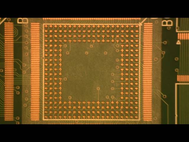
In this era of electronics miniaturization, high yield and low-cost integrated circuit (IC) substrates play a crucial role by providing a reliable method of high density interconnection of chip to board. In order to maximize substrate real-estate, the distance between Cu traces also known as line and space (L/S) should be minimized. Typical PCB technology consists of L/S larger than 40 µ whereas more advanced wafer level technology currently sits at or around 2 µm L/S. In the past decade, the chip size has decreased significantly along with the L/S on the substrate. The decreasing chip scales and smaller L/S distances has created unique challenges for both printed circuit board (PCB) industry and the semiconductor industry. Fan-out panel-level packaging (FOPLP) is a new manufacturing technology that seeks to bring the PCB world and IC/semiconductor world even closer. While FOPLP is still an emerging technology, the amount of high-volume production in this market space provide a financial incentive to develop innovative solutions in order to enable its ramp up. The most important performance aspect of the fine line plating in this market space is plating uniformity or planarity. Plating uniformity, trace/via top planarity, which measures how flat the top of the traces and vias are a few major features. This is especially important in multilayer processing, as nonuniformity on a lower layer can be transferred to successive layers, disrupting the device design with catastrophic consequences such as short circuits. Additionally, a non-planar surface could also result in signal transmission loss by distortion of the connecting points, like vias and traces. Therefore, plating solutions that provide a uniform, planar profile without any special post treatment are quite desirable.

Demonstration of BGA rework via stencil printing. BEST's StikNPeel stencil is an adhesive backed stencil which allows users to stick the stencil in to place and simply peel it off the PCB with a temporary adhesive system. This leaves consistent print
Training Courses | | | PCB Design Courses
The PCB design courses teach students the process, techniques and tools needed to design layout of printed circuit boards.
Training Courses | | | PCB Design Courses
The PCB design courses teach students the process, techniques and tools needed to design layout of printed circuit boards.
Events Calendar | Wed Sep 16 18:30:00 UTC 2020 - Wed Sep 16 18:30:00 UTC 2020 | ,
DFM Panel Discussion for PCB Design, Fabrication, and Assembly
Events Calendar | Tue Mar 12 18:30:00 UTC 2024 - Tue Mar 12 18:30:00 UTC 2024 | ,
SMTA Technical Webinar: Translating the Technology, a "Cross-Over" Event - High Reliability
Career Center | Atlanta, Massachusetts USA | Sales/Marketing
Our client is the world leader in automated optical inspection (AOI) systems for use in the manufacture of printed circuit boards (PCB) and flat panel displays (FPD) and is a leader in imaging solutions for PCB production and in AOI systems for use i
Career Center | San Jose, California USA | Engineering
Headquartered in San Jose, as leading PC component distributor and rank #5 DRAM manufacturer in the worldwide, Ma Labs Inc. has specialized in memory modules since 1985. We provide a full range of memory modules from RDRAM, DDR, SD-RAM, SO-DIMM and F
Career Center | Erode, Tamilnadu India | Engineering
Professional Summary 3+ years of experience in the PCB CAM engineering Exposure to FRONTLINE GENESIS 2000 Having exposure in UCAM Exposure to Create, Array & Panelize it for manufacturability Experienced in Creating impedance cou
Career Center | reston, Virginia USA | Engineering,Management,Production,Technical Support
NIGEL COOMBER (703 715 1075) email: ncoomber@yahoo.com OBJECTIVE: To contribute in a position of high responsibility for a progressive technically innovative company which can utilize a highly motivated professional with leading edge experience in a
SMTnet Express, April 10, 2014, Subscribers: 22635, Members: Companies: 13857, Users: 36009 Solar Panel Design Decision and General Information Sheet Alexander L Carrere; iSAT Group This paper is meant to be a guide and a reference to new and old
Heller Industries Inc. | https://hellerindustries.com/parts/591035/
591035 - ELECTRICAL PANEL Phone 1-973-377-6800 Company About News Events New Equipment Convection Reflow Ovens Reflow Oven MK7 -New
| https://pcbasupplies.com/louvered-panel-system-1/
Louvered Panel System Login Create Account Contact View My Cart Menu × Categories Hand Soldering & Rework Soldering Robots Pick


