
Industry Directory | Consultant / Service Provider / Media / Publisher / Online Resource / Other
PCB Libraries' "Footprint Expert" suite uses CAD LEAP(tm) Technology to greatly simplify footprint and 3D STEP model creation; it is used by tens of thousands of PCB designers and engineers all over the world.
New Equipment | Education/Training
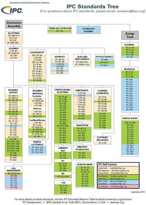
IPC standards, the results of industry consensus and collaboration, are respected throughout the whole world. Using IPC standards allows manufacturers, customers and suppliers to speak the same language. IPC standards are used by the electronics

The PCB Footprint Expert is a powerful CAD library development tool powered by our own proprietary CAD LEAP Technology (Libraries Enhanced with Automated Preferences). It is packed with very powerful advanced library management features that cuts foo
Electronics Forum | Tue Oct 30 08:48:01 EST 2001 | dougie
Hi, Our PCB designers are beginning to send up designs to manufacturing that have increasingly difficult footprints to work with. The footprints have been generated by the IPC-SM-782 calculator but just look wrong to me. The pitch of the devices in
Electronics Forum | Thu Sep 09 09:13:10 EDT 1999 | Scott Cook
| hi, i m college student. i m currently doing my Final year project in PCB drilling. the main task is to design auto feeder which allign the PCB properly in position before drilling take place. the close tolerance becomes a big problem to the precis
Used SMT Equipment | In-Circuit Testers
0.5 UI calibrated, compliant and integrated jitter injection: RJ, RJ-LF, RJ-HF, PJ1, PJ2, SJ, BUJ, ISI, sinusoidal interference, triangular and arbitrary SSC and residual SSC Excellent signal performance and sensitivity Built-in clock data

Used SMT Equipment | In-Circuit Testers
0.5 UI calibrated, compliant and integrated jitter injection: RJ, RJ-LF, RJ-HF, PJ1, PJ2, SJ, BUJ, ISI, sinusoidal interference, triangular and arbitrary SSC and residual SSC Excellent signal performance and sensitivity Built-in clock data
Industry News | 2018-10-18 11:21:46.0
Designing a Multilayer PCB Layout
Industry News | 2017-05-16 17:59:37.0
PCB Technology Trends 2016, a global study published this month by IPC – Association Connecting Electronics Industries®, is now available. The survey-based study shows how printed circuit board (PCB) manufacturers are meeting today’s technology demands and looks at the changes expected by 2021 that will affect the whole industry.
Technical Library | 2019-09-11 23:33:04.0
There are numerous techniques to singulate printed circuit boards after assembly including break-out, routing, wheel cutting and now laser cutting. Lasers have several desirable advantages such as very narrow kerf widths as well as virtually no dust, no mechanical stress, visual pattern recognition and fast set-up changes. The very narrow kerf width resulting from laser ablation and the very tight tolerance of the cutting path placement allows for more usable space on the panel. However, the energy used in the laser cutting process can also create unwanted products on the cut walls as a result of the direct laser ablation. The question raised often is: What are these products, and how far can the creation of such products be mitigated through variation of the laser cutting process, laser parameters and material handling? This paper discusses the type and quantity of the products found on sidewalls of laser depaneled circuit boards and it quantifies the results through measurements of breakdown voltage, as well as electrical impedance. Further this paper discusses mitigation strategies to prevent or limit the amount of change in surface quality as a result of the laser cutting process. Depending on the final application of the circuit board it may prompt a need for proper specification of the expected results in terms of cut surface quality. This in turn will impact the placement of runs and components during layout. It will assist designers and engineers in defining these parameters sufficiently in order to have a predictable quality of the circuit boards after depaneling.

IPC Vice President David Bergman explains where to find and how to use the Document Revision Table.

The PCB Footprint Expert is a powerful CAD library development tool powered by our own proprietary CAD LEAP Technology (Libraries Enhanced with Automated Preferences). It is packed with very powerful advanced library management features that cuts foo
Career Center | Riyadh 11623, Philippines | Engineering,Maintenance,Production
PROFESSIONAL EXPERIENCE: Connected in the field of manufacturing/electronics industry experienced in the line, Through Hole and Surface Mount Technology, worked on various Fuji Machines Universal model, such as: CP 643E chip shooter QP 242E chip mou
PCB Libraries, Inc. | https://www.pcblibraries.com/Forum/topic2858&OB=DESC.html
1008 Chip Inductor Land Pattern - PCB Libraries Forum Forum Home > Libraries > Footprints / Land Patterns New Posts FAQ Search Events Register Login 1008 Chip Inductor Land Pattern
GPD Global | https://www.gpd-global.com/co_website/pdf/doc/FLOware-Software-Guide-Addendum-Deferred-Reverse.pdf
. Pattern Name Name of the pattern used with this valve/tool. This name can be up to 24 characters long. Auto Clean Activates or deactivates automatic needle cleaning at the material level, making the Auto Clean setting the default in every program using the current material


