New Equipment | Assembly Services
Parameter name / model specification / type UL330 UL445 UL530 UL535 Supply voltagePower Supply: AC220V/50/60HZ Supply pressureAir Supply: 5kgf/c㎡ PCB size (mm): 330*50~250 445*50~330 530*50~390 535*50~460 PCB direction: Left to right( opetio
New Equipment | Board Handling - Conveyors
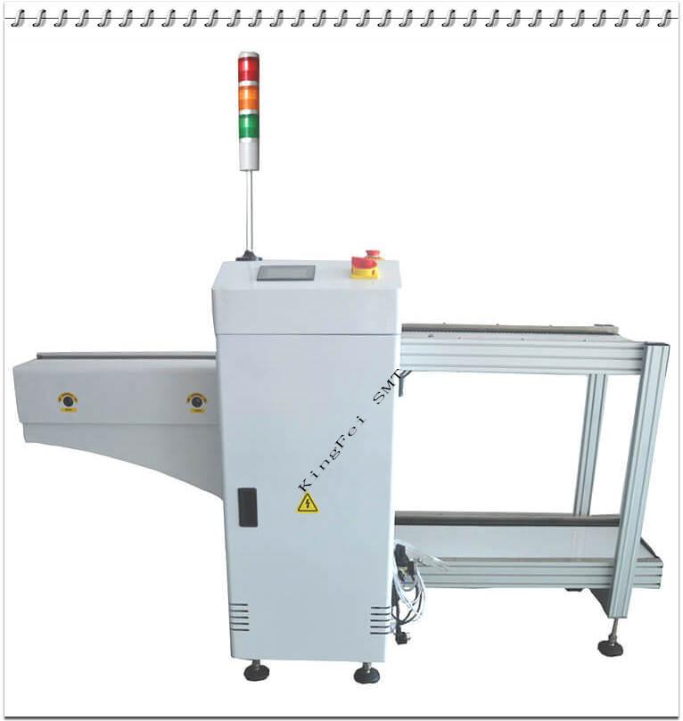
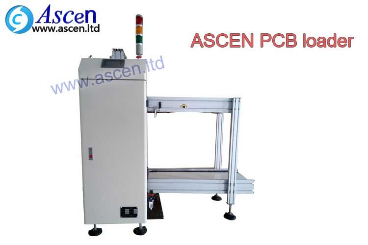
auto pcb magazine loader and SMT multi magazine loader as SMT line automatic PCB magazine loader that feeds PCBs into the Process Line from Stacks or Magazines.The unit loads the production line automatically by pushing PCBA out of a magazine onto th
Electronics Forum | Thu Sep 05 23:18:03 EDT 2013 | feiyangniao
There is a new toy I received today: a NeoDen TM-240A automatic desktop pick and place machine! I’ve kept my eyes on this baby for a quite a while, and finally decided to make a purchase last week. The shipping was very fast: DHL from China, a total
Electronics Forum | Wed Jul 24 09:54:49 EDT 2019 | amitthepcbguy
Typically, the reliability of PCBs suffers significantly due to the increase in aspect ratio. It is not preferred to opt for high thickness boards. However, I would like to point out that your assumption seems to be wrong as board layers do not direc

Used SMT Equipment | Chipshooters / Chip Mounters
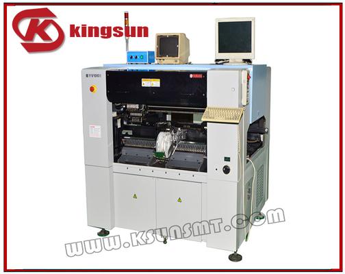
Product name: YV100X YAMAHA multi-functional chip mounter Product number: YV100X Products in detail YAMAHA multi-function placement machineYAMAHA YV100X substrate size: ATS20 (end to put) W -AT assembly: L460 * W250 (Max)/L50 * W50 (Min)sub
Used SMT Equipment | Pick and Place/Feeders
Yamaha YV100ll pick and place machine Product name: YV100 Ⅱ YAMAHAmulti-functional chip mounter Product number: YV100 Ⅱ Products in detail YAMAHA multi-function chip mounter YAMAHA YV100II The brand YAMAHA model YV100 - II Automatic manua
Industry News | 2003-03-11 08:45:00.0
CAMtastic DXP is the latest version of Altium's complete CAM verification and editing system that bridges the gap between PCB design and manufacturing and facilitates communication between board designers, fabrication engineers, and their clients.
Industry News | 2003-04-11 08:53:18.0
This agreement establishes PCS as the exclusive representative of RSI in the UK and the Republic of Ireland.

Parts & Supplies | Other Equipment
We're highly specialized in repair service of JUKI CPU ,SUB-CPU ,laser boared,X/Y/Z/Q driver,24V power card,head card,image card,I/O card,XMP card ,MTC card Etc. You can send inquiry directly to fhysmt at hysmt dot cn JUKI 700/2000 board: E86067250
Technical Library | 2023-07-25 16:42:54.0
Printing solder paste for very small components like .3mm pitch CSP's and 01005 Chip Components is a challenge for the printing process when other larger components like RF shields, SMT Connectors, and large chip or resistor components are also present on the PCB. The smaller components require a stencil thickness typically of 3 mils (75u) to keep the Area Ratio greater than .55 for good paste transfer efficiency. The larger components require either more solder paste height or volume, thus a stencil thickness in the range of 4 to 5 mils (100 to 125u). This paper will explore two stencil solutions to solve this dilemma. The first is a "Two Print Stencil" option where the small component apertures are printed with a thin stencil and the larger components with a thicker stencil with relief pockets for the first print. Successful prints with Keep-Outs as small as 15 mils (400u) will be demonstrated. The second solution is a stencil technology that will provide good paste transfer efficiency for Area Ratio's below .5. In this case a thicker stencil can be utilized to print all components. Paste transfer results for several different stencil types including Laser-Cut Fine Grain stainless steel, Laser-Cut stainless steel with and w/o PTFE Teflon coating, AMTX E-FAB with and w/o PTFE coating for Area Ratios ranging from .4 up to .69.
Technical Library | 2020-08-27 01:22:45.0
Initially adopted internal specifications for acceptance of printed circuit boards (PCBs) used for wire bonding was that there were no nodules or scratches allowed on the wirebond pads when inspected under 20X magnification. The nodules and scratches were not defined by measurable dimensions and were considered to be unacceptable if there was any sign of a visual blemish on wire-bondable features. Analysis of the yield at a PCB manufacturer monitored monthly for over two years indicated that the target yield could not be achieved, and the main reasons for yield loss were due to nodules and scratches on the wirebonding pads. The PCB manufacturer attempted to eliminate nodules and scratches. First, a light-scrubbing step was added after electroless copper plating to remove any co-deposited fine particles that acted as a seed for nodules at the time of copper plating. Then, the electrolytic copper plating tank was emptied, fully cleaned, and filtered to eliminate the possibility of co-deposited particles in the electroplating process. Both actions greatly reduced the density of the nodules but did not fully eliminate them. Even though there was only one nodule on any wire-bonding pad, the board was still considered a reject. To reduce scratches on wirebonding pads, the PCB manufacturer utilized foam trays after routing the boards so that they did not make direct contact with other boards. This action significantly reduced the scratches on wire-bonding pads, even though some isolated scratches still appeared from time to time, which caused the boards to be rejected. Even with these significant improvements, the target yield remained unachievable. Another approach was then taken to consider if wire bonding could be successfully performed over nodules and scratches and if there was a dimensional threshold where wire bonding could be successful. A gold ball bonding process called either stand-off-stitch bonding (SSB) or ball-stitch-on-ball bonding (BSOB) was used to determine the effects of nodules and scratches on wire bonds. The dimension of nodules, including height, and the size of scratches, including width, were measured before wire bonding. Wire bonding was then performed directly on various sizes of nodules and scratches on the bonding pad, and the evaluation of wire bonds was conducted using wire pull tests before and after reliability testing. Based on the results of the wire-bonding evaluation, the internal specification for nodules and scratches for wirebondable PCBs was modified to allow nodules and scratches with a certain height and a width limitation compared to initially adopted internal specifications of no nodules and no scratches. Such an approach resulted in improved yield at the PCB manufacturer.
Automatic loader and unloader pcb magazine loader smt loader for smt line APPLICATION: The Single magazine loader is used at the starting of the line for loading of PCB’s to the production line. The unit loads the production line automatically
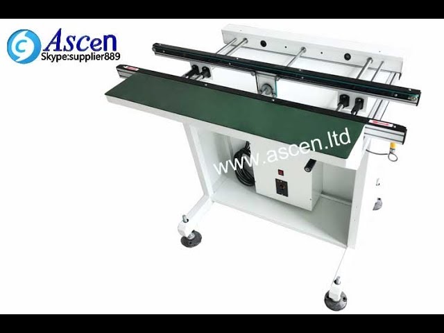
0.5M automatic inspection pcb conveyor and PCB Belt Conveyor|PCB transfer conveyor used for equipment linking, visual inspection, manual assembly, and PCB buffering functions https://www.ascen.ltd/Products/Automatic_SMT_equipment/PCB_conveyor/179.htm
Events Calendar | Tue Mar 30 00:00:00 EDT 2021 - Tue Mar 30 00:00:00 EDT 2021 | ,
Wisconsin Chapter Webinar: PCB Assembly – Labeling and Marking Technology and Materials
SMTnet Express, June 19, 2014, Subscribers: 22851, Members: Companies: 13906, Users: 36363 Anisotropic grain growth and crack propagation in eutectic microstructure under cyclic temperature annealing in flip-chip SnPb composite solder joints Y
| https://www.smtfactory.com/What-is-the-application-prospect-and-development-direction-of-Lyra-Reflow-Oven-id43172477.html
What is the application prospect and development direction of Lyra Reflow Oven? - I.C.T SMT Machine English Bahasa indonesia Сербия Česky Dansk Deutsch
ASCEN Technology | https://www.ascen.ltd/Products/PCB_depaneling_machine/1070.html
: It can use for following type PCB panel with V-cut of vertical and horizontal direction: Please check the following video to check this customized PCB depaneling machine how to process these complex PCB panel

Products, services, training & consulting for the assembly, rework & repair of electronic assemblies. BGA process experts. Manufacturers Rep, Distributor & Service Provider for Seamark/Zhuomao and Shuttle Star BGA Rework Stations.
Training Provider / Manufacturer's Representative / Equipment Dealer / Broker / Auctions / Consultant / Service Provider
1750 Mitchell Ave.
Oroville, CA USA
Phone: (888) 406-2830


