Industry Directory | Manufacturer
professional manufacturer of pcb
Industry News | 2018-10-18 09:06:41.0
Gold Fingers: A Guide to Understanding Gold-Plated PCB Connectors
New Equipment | Fabrication Services
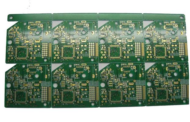
Low Cost Heavy Copper PCB China 4 Layers Circuit Boards Supplier Quick Details: FR4 base material 1.6mm board thickness 2oz heavy copper Plating gold finishing RF custom PCB boards Used for Radio Frequency From China PCB manufacturer Specifications
We are electronic contract manufacture and we also have JIT facility. Our head office located in Markham, Ontario, Canada. We do have a facility in USA, MEXICO and BRAZIL.
Technical Library | 2020-08-27 01:22:45.0
Initially adopted internal specifications for acceptance of printed circuit boards (PCBs) used for wire bonding was that there were no nodules or scratches allowed on the wirebond pads when inspected under 20X magnification. The nodules and scratches were not defined by measurable dimensions and were considered to be unacceptable if there was any sign of a visual blemish on wire-bondable features. Analysis of the yield at a PCB manufacturer monitored monthly for over two years indicated that the target yield could not be achieved, and the main reasons for yield loss were due to nodules and scratches on the wirebonding pads. The PCB manufacturer attempted to eliminate nodules and scratches. First, a light-scrubbing step was added after electroless copper plating to remove any co-deposited fine particles that acted as a seed for nodules at the time of copper plating. Then, the electrolytic copper plating tank was emptied, fully cleaned, and filtered to eliminate the possibility of co-deposited particles in the electroplating process. Both actions greatly reduced the density of the nodules but did not fully eliminate them. Even though there was only one nodule on any wire-bonding pad, the board was still considered a reject. To reduce scratches on wirebonding pads, the PCB manufacturer utilized foam trays after routing the boards so that they did not make direct contact with other boards. This action significantly reduced the scratches on wire-bonding pads, even though some isolated scratches still appeared from time to time, which caused the boards to be rejected. Even with these significant improvements, the target yield remained unachievable. Another approach was then taken to consider if wire bonding could be successfully performed over nodules and scratches and if there was a dimensional threshold where wire bonding could be successful. A gold ball bonding process called either stand-off-stitch bonding (SSB) or ball-stitch-on-ball bonding (BSOB) was used to determine the effects of nodules and scratches on wire bonds. The dimension of nodules, including height, and the size of scratches, including width, were measured before wire bonding. Wire bonding was then performed directly on various sizes of nodules and scratches on the bonding pad, and the evaluation of wire bonds was conducted using wire pull tests before and after reliability testing. Based on the results of the wire-bonding evaluation, the internal specification for nodules and scratches for wirebondable PCBs was modified to allow nodules and scratches with a certain height and a width limitation compared to initially adopted internal specifications of no nodules and no scratches. Such an approach resulted in improved yield at the PCB manufacturer.
Industry News | 2003-04-22 08:10:17.0
EAO introduces the 1K2, a superior quality changeover slide switch recommended for PCB configuration applications. The products is recommended for PCB configuration applications and occupies a board space measuring only 10mm x 2.5mm with a height of 4.5mm excluding actuator.
Industry News | 2020-02-05 12:30:26.0
This intelligent measurement tool is a new type of handheld LCR meter that can quickly test, identify, and measure board-mounted surface-mount and leaded devices without the need to remove them from a circuit board.
Industry News | 2019-11-05 22:19:03.0
> News-Blog > Guideline for wire bonding Guideline for wire bonding Tuesday,Jun 12,2018 There are two wire bonding processes that are used, Thermosonic (T/S) Gold Ball Wire Bonding and Ultrasonic (U/S) Aluminum Wedge Wire Bonding. Approximately 90% of all IC Assembly in Semiconductor Packages is manufactured using Gold Ball Bonding process, while Aluminum Wedge Bonding is used to produce about 10% of other Wire Bonding requirements on Printed Circuit Boards (PCB), Printed Circuit Flex (PCF) and other Packages.
.jpg)
Parts & Supplies | Pick and Place/Feeders
FUJI NXT V12 SHEET 2MGKHA035100 PS03562 We are supply Smt Machine Spare Parts for Panasonic, Yamaha, i-Pluse, JUKI, Fuji, Samsung, Sony, Universal… Such as Smt machine feeders, Nozzles, Drivers, Motors, Filter, Valve, PCB Board, Cylinder… And AI
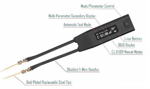
New Equipment | Test Equipment
Smart Tweezers ST-5S are the newest model in the Smart Tweezers line of handheld LCR-meters. This model will be replacing the previous ST-5 model. Smart Tweezers are a fully automatic, handheld, digital LCR-meter designed specifically for evaluating

Products, services, training & consulting for the assembly, rework & repair of electronic assemblies. BGA process experts. Manufacturers Rep, Distributor & Service Provider for Seamark/Zhuomao and Shuttle Star BGA Rework Stations.
Training Provider / Manufacturer's Representative / Equipment Dealer / Broker / Auctions / Consultant / Service Provider
1750 Mitchell Ave.
Oroville, CA USA
Phone: (888) 406-2830


