Technical Library | 2020-01-01 17:06:52.0
The majority of electronic failures occur due to thermally induced stresses and strains caused by excessive differences in coefficients of thermal expansion (CTE) across materials.CTE mismatches occur in both 1st and 2nd level interconnects in electronics assemblies. 1st level interconnects connect the die to a substrate. This substrate can be underfilled so there are both global and local CTE mismatches to consider. 2nd level interconnects connect the substrate, or package, to the printed circuit board (PCB). This would be considered a "board level" CTE mismatch. Several stress and strain mitigation techniques exist including the use of conformal coating.
Technical Library | 2015-04-29 03:48:39.0
SPI equipment is routinely used in Printed Circuit Board (PCB) manufacturing to monitor and control one of the most crucial steps affecting the finished quality of circuit board. Solder paste deposition is the key process in board assembly operations using SMT techniques. Our LSM™ system was the industry's first popular method of manually inspecting solder paste; our SE systems revolutionized SMT production by offering an automated method for performing in-process 3D inspection on the assembly line. SPI systems measure the height and volume of the solder pads before the components are applied and the solder melted, and when used properly, can reduce the incidence of solder-related defects to statistically insignificant amounts. Critical to the SPI measurement is the accuracy of the height measurement because that has a direct correlation with solder volume and defects.
Technical Library | 2021-09-29 13:35:21.0
In PCB circuit assemblies the trend is moving to more SMD components with finer pitch connections. The majority of the assemblies still have a small amount of through hole (THT) components. Some of them can't withstand high reflow temperatures, while others are there because of their mechanical robustness. In automotive applications these THT components are also present. Many products for cars, including steering units, radio and navigation, and air compressors also use THT technology to connect board-to-board, PCB's to metal shields or housings out of plastic or even aluminium. This is not a simple 2D plain soldering technology, as it requires handling, efficient thermal heating and handling of heavy (up to 10 kg) parts. Soldering technology becomes more 3D where connections have to be made on different levels. For this technology robots using solder wire fail because of the spattering of the flux in the wires and the long cycle time. In wave soldering using pallets the wave height is limited and pin in paste reflow is only a 2D application with space limitations. Selective soldering using dedicated plates with nozzles on the solder area is the preferred way to make these connections. All joints can be soldered in one dip resulting in short cycle times. Additional soldering on a small select nozzle can make the system even more flexible. The soldering can only be successful when there is enough thermal heat in the assembly before the solder touches the board. A forced convection preheat is a must for many applications to bring enough heat into the metal and board materials. The challenge in a dip soldering process is to get a sufficient hole fill without bridging and minimize the number of solder balls. A new cover was designed to improve the nitrogen environment. Reducing oxygen levels benefits the wetting, but increases the risk for solder balling. Previous investigations showed that solder balling can be minimized by selecting proper materials for solder resist and flux.
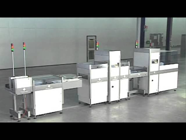
Industry News | 2006-07-05 08:05:43.0
Achieves Shortened Time-to-Market
Industry News | 2018-12-10 18:01:46.0
Our Italian colleagues and Latin scholars will know that the letter ‘D’ is the Roman numeral for 500. Right now, on the Europlacer manufacturing floor in Rocheserviere in France, the production team is preparing to build our 500th iineo placement machine.
Successful manufacturing requires that the materials are in the right place Just on Time. Our board handling products are known for high quality, even our first PCB handling products from early 90’s are still used in many factories around the world.
Technical Library | 2020-09-02 22:02:13.0
With the adoption of Wafer Level Packages (WLP) in the latest generation mobile handsets, the Printed Circuit Board (PCB) industry has also seen the initial steps of High Density Interconnect (HDI) products migrating away from the current subtractive processes towards a more technically adept technique, based on an advanced modified Semi Additive Process (amSAP). This pattern plate process enables line and space features in the region of 20um to be produced, in combination with fully filled, laser formed microvias. However, in order to achieve these process demands, a step change in the performance of the chemical processes used for metallization of the microvia is essential. In the electroless Copper process, the critical activator step often risks cross contamination by the preceding chemistries. Such events can lead to uncontrolled buildup of Palladium rich residues on the panel surface, which can subsequently inhibit etching and lead to short circuits between the final traces. In addition, with more demands being placed on the microvia, the need for a high uniformity Copper layer has become paramount, unfortunately, as microvia shape is often far from ideal, the deposition or "throw" characteristics of the Copper bath itself are also of critical importance. This "high throwing power" is influential elsewhere in the amSAP technique, as it leads to a thinner surface Copper layer, which aids the etching process and enables the ultra-fine features being demanded by today's high end PCB applications. This paper discusses the performance of an electroless Copper plating process that has been developed to satisfy the needs of challenging amSAP applications. Through the use of a radical predip chemistry, the formation, build up and deposition of uncontrolled Pd residues arising from activator contamination has been virtually eradicated. With the adoption of a high throwing power Copper bath, sub 30um features are enabled and microvia coverage is shown to be greatly improved, even in complex via shapes which would otherwise suffer from uneven coverage and risk premature failure in service. Through a mixture of development and production data, this paper aims to highlight the benefits and robust performance of the new electroless Copper process for amSAP applications


Products, services, training & consulting for the assembly, rework & repair of electronic assemblies. BGA process experts. Manufacturers Rep, Distributor & Service Provider for Seamark/Zhuomao and Shuttle Star BGA Rework Stations.
Training Provider / Manufacturer's Representative / Equipment Dealer / Broker / Auctions / Consultant / Service Provider
1750 Mitchell Ave.
Oroville, CA USA
Phone: (888) 406-2830


