Industry Directory | Manufacturer
phoenix|x-ray manufactures microfocus X-ray systems and provides system maintenance plus inspection services. Systems come with an open or closed tube and are dedicated to the pcba, package and multilayer industries.
Industry Directory | Equipment Dealer / Broker / Auctions
Service and sales for DEK printer,Phoenix X-RAY,Vitronics Reflow Oven
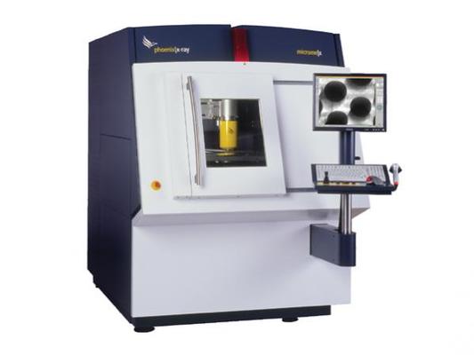
The phoenix microme|x is a high-resolution 180 kV microfocus X-ray inspection system for real time inspection of solder joints and electronic components as well as for automated inspection (µAXI). Innovative and unique features and an extreme high po
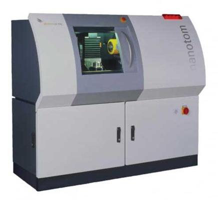
GE's phoenix nanotom® s is the first 180 kV/15 W nanofocus computed tomography (nano ct) system perfectly tailored to applications e.g. in material science, precision injection moulding or micromechanics. The nanotom® is the inspection solution for
Electronics Forum | Tue Jan 09 11:04:01 EST 2024 | micropak
Hi Anyone happen to have service manuals (level 1 & 2) for GE/Phoenix X-Ray ? Particularly looking for X-Ray tube service information.
Electronics Forum | Sat Mar 13 13:34:45 EST 2021 | proy
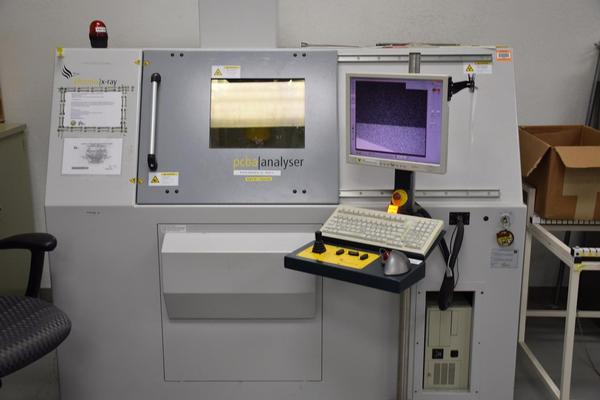
I have an excellent operating X-Ray - Phoenix PCB analyser 160. It seems there was available software for Voiding Calculation but I am not sure if my machine has this - I do know that we have the BGA analysis tool, but have to look in and see if we
Used SMT Equipment | X-Ray Inspection
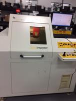
Make: GE Model: Pcba ! Inspector 100 Vintage: 2001 Description: X-Ray System Condition: Complete & Fully Operational Video Link: https://www.dropbox.com/sh/fjlezf9qjfciszo/AACWw8hheYZYMg1mo-1tllkSa?dl=0 Location: Texas Availability: Immediate
Used SMT Equipment | X-Ray Inspection
This equipment is located in our upcoming Nypro / Jabil Online Auction. Please select the below link for more details. http://bajabid.com/online-smt-auction-featuring-items-nypro/
Industry News | 2008-08-14 14:03:27.0
San Jose, CA � This year's fifth annual International Wafer-Level Packaging Conference (IWLPC), October 13-16, will be the largest ever, according to Dr. Ken Gilleo, IWLPC general chair.
Industry News | 2018-12-08 03:22:25.0
Electronic Components, Parts and Their Function
Technical Library | 2021-11-03 17:05:39.0
Additively printed circuits provide advantages in reduced waste, rapid prototyping, and versatile flexible substrate choices relative to conventional circuit printing. Copper (Cu) based inks along with intense pulsed light (IPL) sintering can be used in additive circuit printing. However, IPL sintered Cu typically suffer from poor solderability due to high roughness and porosity. To address this, hybrid Cu ink which consists of Cu precursor/nanoparticle was formulated to seed Cu species and fill voids in the sintered structure. Nickel (Ni) electroplating was utilized to further improve surface solderability. Simulations were performed at various electroplating conditions and Cu cathode surface roughness using the multi-physics finite element method. By utilizing a mask during IPL sintering, conductivity was induced in exposed regions; this was utilized to achieve selective Ni-electroplating. Surface morphology and cross section analysis of the electrodes were observed through scanning electron microscopy and a 3D optical profilometer. Energy dispersive X-ray spectroscopy analysis was conducted to investigate changes in surface compositions. ASTM D3359 adhesion testing was performed to examine the adhesion between the electrode and substrate. Solder-electrode shear tests were investigated with a tensile tester to observe the shear strength between solder and electrodes. By utilizing Cu precursors and novel multifaceted approach of IPL sintering, a robust and solderable Ni electroplated conductive Cu printed electrode was achieved.
Career Center | san diego,, California USA | Engineering,Production,Quality Control,Technical Support
SMT Process Engineer, ISO-9001, IPC-600/610/620/7711/7721, J-STD-001, Thermal profiling, Lean manufacturing.
Career Center | Ballston Spa, New York USA | Engineering,Maintenance,Production,Purchasing,Quality Control,Research and Development,Sales/Marketing,Technical Support
Qualifications / Skills: Maintain and repair X-Ray inspection equipment Maintain Surface Mount Manufacturing Systems Full DEK OEM equipment training Train Surface Mount Technology, Semiconductor, and Solar Photovoltaic operators and engineers Mainta
ASYMTEK Products | Nordson Electronics Solutions | https://www.nordson.com/en/divisions/dage/about/news/nordson-dage-rxpands-into-new-research-and-development-facility
Nordson DAGE Rxpands into New Research and Development Facility X-Ray Inspection and Test Products Corporate | Global Directory | Languages Division Only All of Nordson Home Products Bondtesting Systems Micro Materials Testing Wafer Inspection and Metrology X-ray Inspection Systems X-ray Counting Systems Applications Battery
| https://www.smtfactory.com/smt-production-lines.html
& Unloaders Conveyors Traffic Controllers Buffers Vision Inspection Equipment AOI / Automatic Optical Machine SPI / Solder Paste Inspection AXI / Automatic X-Ray Inspection SMT Stencil Inspection

.gif)


