
This video describes the IPC A-600 training and certification program. The IPC A-600 specification is a set of acceptability specifications for printed circuit boards. These standards determine the acceptance and reject criteria for printed wiring bo
This video describes the IPC A-600 training and certification program. The IPC A-600 specification is a set of acceptability specifications for printed circuit boards. These standards determine the acceptance and reject criteria for printed wiring bo
This video describes the IPC A-600 training and certification program. The IPC A-600 specification is a set of acceptability specifications for printed circuit boards. These standards determine the acceptance and reject criteria for printed wiring bo
This video describes the IPC A-600 training and certification program. The IPC A-600 specification is a set of acceptability specifications for printed circuit boards. These standards determine the acceptance and reject criteria for printed wiring bo
Industry Directory | Manufacturer
Hi-Rel Thick Film Substrates, Multilayer, Thru-Hole/Edge Around, 2mil Lines Etched Conductors
Multilayer Circuit- MHD provides simple single layer circuits to complex high density, thru-hole multilayer circuits. MHD's Thick Film Substrates are used in various applications: Microwave, Medical, Military, Aerospace, Automotive and Commercial.
Technical Library | 2023-11-14 19:52:11.0
The continuous drive in the Electronics industry to build new and innovative products has caused competitive design companies to develop assemblies with consolidated PCB designs, decreased physical sizes, and increased performance characteristics. As a result of these new designs, manufacturers of electronics are forced to contend with many challenges. One of the most significant challenges being the processing of thru-hole components on high thermal mass PCBs having the potential to exceed 20 layers in thicknesses and have copper mass contents of over 40oz. High thermal mass PCBs, coupled with the use of mixed technologies, decreased component spacing, and the change from Tin Lead Solder to Lead Free Alloys has lead many manufacturing facilities to purchase advanced soldering equipment to process challenging assemblies with a high degree of repeatability.
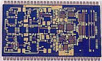
Layer: 8 layers Material: FR-4 Board Thickness: 0.6mm Surface Finish: Immersion Gold 1~4u Copper Thickness: 1/3 oz Impedance, 4/4mils width/spacing Layers: 2--36layers Max manufacturing size: 640mm*1100mm Copper foil thickness: 0.5OZ-13OZ M

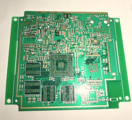
Layer: 2 Material: FR-4 Board Thickness: 1.6mm Surface Finish: HAL Copper Thickness: 2/2 oz Green Solder Mask Layers: 2--36layers Max manufacturing size: 640mm*1100mm Copper foil thickness: 0.5OZ-13OZ Min line width/space: 3mil/3mil Min
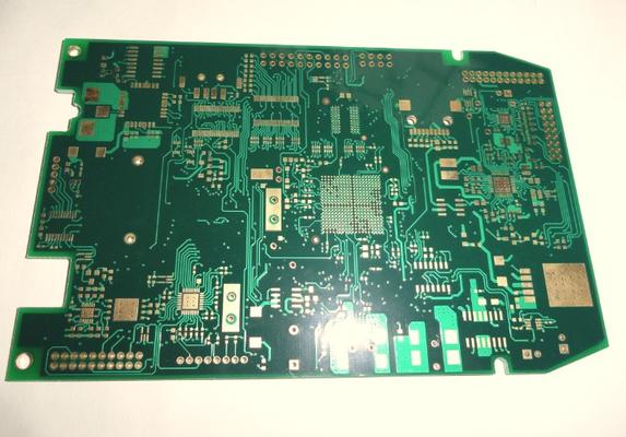
Layer: 6 layers Material: FR-4 Board Thickness: 1.0mm Surface Finish:ENIG Copper Thickness: 1 oz all layers Blind via L1~L2 and L1~L3 Layers: 2--36layers Max manufacturing size: 640mm*1100mm Copper foil thickness: 0.5OZ-13OZ Min line width


