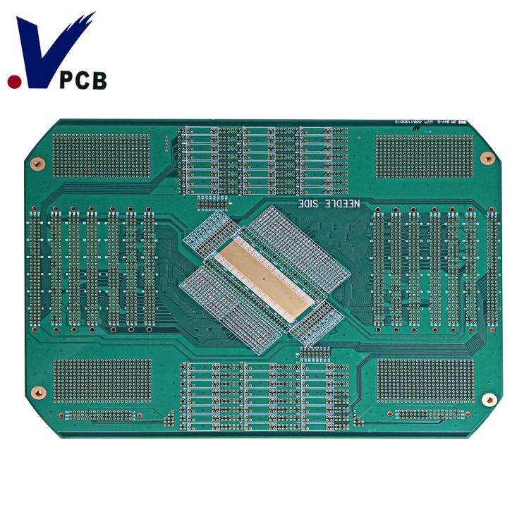
Manufacture capability Layers: 1-16 layers Materials: CEM1, CEM3, Teflon, Rogers,FR-4, High Tg FR-4, Aluminum Base, Halogen Free Max. Board Size: 510*1200mm Material: RoHS Directive-compliant PCB thickness: 1.6 ±0.1mm Out Layer Copper Thickn
Industry Directory | Manufacturer
We provide cost effective, custom printed circuit boards (PCBs) through an instant online system. We also provide PCB Assemb
Training Courses | | | IPC-600 Specialist (CIS)
The Certified IPC-600 Specialist (CIS) training targets quality assurance and acceptance of bare printed circuit boards.
Training Courses | | | IPC-600 Specialist (CIS)
The Certified IPC-600 Specialist (CIS) training targets quality assurance and acceptance of bare printed circuit boards.
Training Courses | | | IPC-600 Trainer (CIT)
The Certified IPC-600 Trainer (CIT) courses recognize individuals as qualified trainers in the area of quality assurance of bare printed circuit boards and prepare them to deliver Certified IPC-600 (CIS) training.
New Equipment | Assembly Services
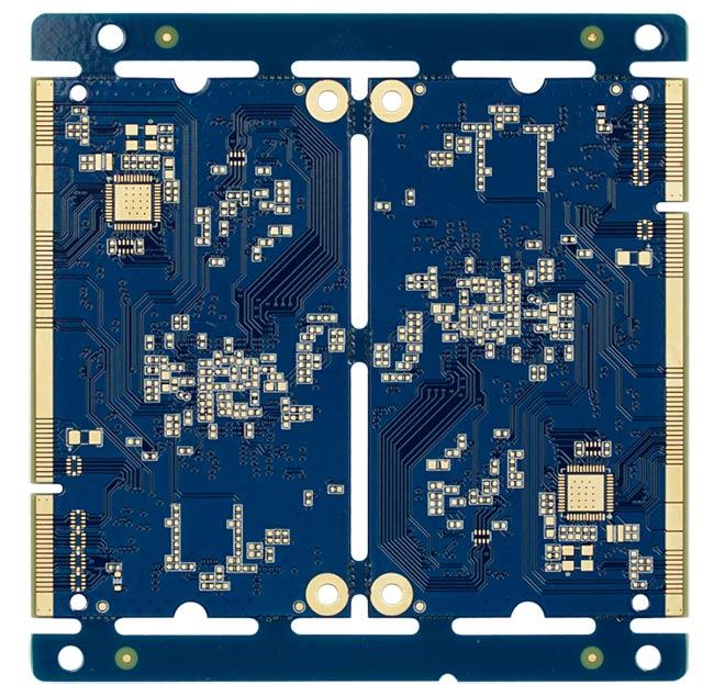
Thick-Copper PCB Material: Fr-4 Layer Count: 4 layers PCB Thickness: 1.4mm Min. Trace / Space Outer: 0.065mm Min. Drilled Hole: 0.2mm Via Process: Tenting Vias Surface Finish: ENIG Product Features Features: 1) Years of experience in half-
New Equipment | Assembly Services
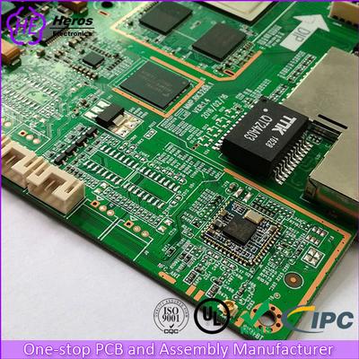
One-stop PCB and Assembly Manufacturers Specialized in one-stop PCB and Assembly manufacturing, Heros Electronics is committed to providing quick-turn high quality custom PCB and smt assembly to our customers all over the world with affordable pri
.jpg)
New Equipment | Assembly Services
One-stop PCB and Assembly Manufacturers Specialized in one-stop PCB and Assembly manufacturing, Heros Electronics is committed to providing quick-turn high quality custom PCB and smt assembly to our customers all over the world with affordable pri
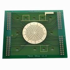
General specification for Microwave/RF PCB Layer count: 1-6 Board thickness: 0.2-3.2mm Copper thickness: 0.5-4oz Dielectric Constant(DK): 2.2-10.3 Min trace width/spacing: 4/4mil Min drill hole size: 0.2mm Surface treatment: HAL(Lead free), I
With the development of miniaturization of assembly components, the layout area and pattern design area of PCBs have also been continuously reduced, and PCB manufacturers are constantly updating the production process to conform to the development tr


.png)
