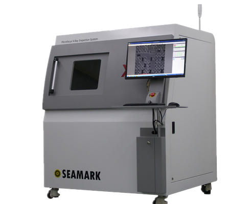
Major applications: PCBA BGA/IC LED Aliminum die casting Battery connector inspecting 1. Semiconductor package 2. Electronic connector module. 3. Original Package 4. Aerospace components 5. Medical appliances 6. Automation components X-ray In
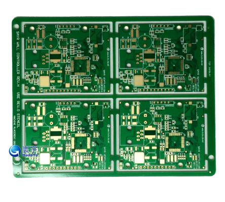
Item Capability Number of Layers 2 layer Quantity :3Panel Material FR4 PCB Thickness 1.6mm Copper Thickness 1/1 OZ Max Finish size 580X610mm Min. Hole size Min: 0
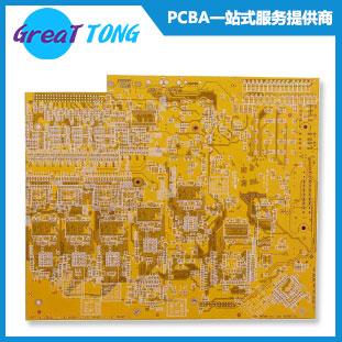
Supplier: Shenzhen Grande Electronics Layers: 4 Application: Stone Crusher PCB Prototype and Manufacturing Process | Grande PCB & PCBA PCB Parameter: FR-4/HTG150 Thickness: 1.6mm Surface Treatment: ENIG Testing: 100% E-test Package: Vacuum packing L
New Equipment | Board Handling - Pallets,Carriers,Fixtures
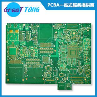
Supplier: Shenzhen Grande Electronics Layers: 4 Application: Grande - Automobile PCB Prototyping and Manufacturing PCB Parameter: FR-4/HTG150 Thickness: 1.6mm Surface Treatment: ENIG Testing: 100% E-test Package: Vacuum packing Lead Time: 10-15 da

New Equipment | Board Handling - Storage
Supplier: Grande Electronics Layers: 4 Application: Pager Electronic Manufacturing | Fusion PCB Fabrication & Prototype PCB Parameter: FR-4/HTG150 Thickness: 1.6mm Surface Treatment: ENIG Testing: 100% E-test Package: Vacuum packing Lead Time: 10-15
Do you have to wipe your stencils after only a few circuit boards? Do you have to spend time at the rework station fixing shorts? Do you pay extra premiums for quick turn stencils? Do you sometimes receive poor quality stencils? ASI has taken the el
Industry News | 2018-10-18 10:16:53.0
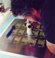
Solder Tinned Pads vs Gold Plated Pads - The Importance of Selecting the Proper Surface Finish
Technical Library | 2013-03-27 23:43:40.0
Vapor phase, once cast to the annals’ of history is making a comeback. Why? Reflow technology is well developed and has served the industry for many years, it is simple and it is consistent. All points are true – when dealing with the centre section of the bell curve. Today’s PCB manufacturers are faced with many designs which no longer fall into that polite category but rather test the process engineering groups with heavier and larger panels, large ground planes located in tricky places, component mass densities which are poorly distributed, ever changing Pb Free alloys and higher process temperatures. All the time the costs for the panels increase, availability of “process trial” boards diminishes and yields are expected to be extremely high with zero scrap rates. The final process in the assembly line has the capacity to secure all the value of the assembly or destroy it. If a panel is poorly soldered due to poor Oven setup or incorrect programming of the profile the recovery of the panel is at best expensive, at worst a loss. For these challenges people are turning to Vapor Phase.
New Equipment | Board Handling - Pallets,Carriers,Fixtures
Time and temperature are very important variables in soldering printed circuit boards. It is important to bring the circuit board assemblies up to a high enough temperature for a long enough period to effectively solder the components to the board. G


