New Equipment | Rework & Repair Services
STI has qualified technicians trained in IPC 7711/7721, as well as in custom design solutions, to address your electronic rework and repair needs. STI’s services encompass both mainstream assembly technologies (surface mount and through-hole) as well
Henkel offers innovative capillary flow underfill encapsulants for flip-chip, CSP and BGA devices. These are highly flowable, high purity, onecomponent encapsulants. They form a uniform and void-free underfill layer to improve reliability performance

This video describes the IPC A-600 training and certification program. The IPC A-600 specification is a set of acceptability specifications for printed circuit boards. These standards determine the acceptance and reject criteria for printed wiring bo
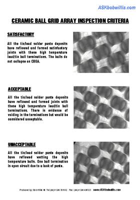
Ball Grid Array X-Ray Inspection Guide - 20 Colour Charts Includes X-Ray inspection guide of satisfactory BGA solder joints and process defects, x-ray images are black and white. The posters are provided as a pdf file and can be printed as A4 or A3
New Equipment | Assembly Services
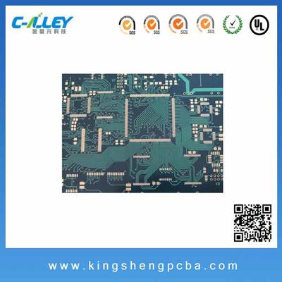
Our Service PCB Assembly and PCB&PCBA design are our main business.We are able to undertake a high quality Printed Circuit Board Assembly on competitive prices and flexible conditions.We are a complete “One- Stop” resource for printed circuit board
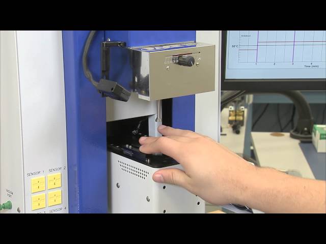
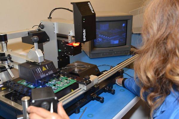
"The IR 3000 offers advanced surface mount rework capability in an integrated, cost-effective, bench-top work station." This video covers the basic processes of the IR 3000, focusing primarily on: Installations, Removals, Component Alignment and Ins
New Equipment | Fabrication Services
Our Service PCB Assembly and PCB&PCBA design are our main business.We are able to undertake a high quality Printed Circuit Board Assembly on competitive prices and flexible conditions.We are a complete “One- Stop” resource for printed circuit board
New Equipment | Assembly Services
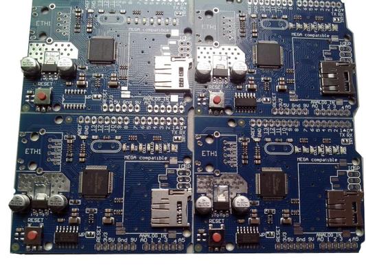
China Double Sided Circuit Boards Fabricaiton and Assembly PCBA Turnkey Manufacturer 2 Layers circuit boards PCB FR4 1.6mm PCB fabrication and assembly 1oz PCB copper thickness Shenzhen PCB and PCBA manufacturer China turnkey contract electroni

Welcome to this Defect of the Month video on head in and on pillow, this series of videos were produced for and featured as part of the NPL/IPC video library and examples are taken from the NPL Defect Database. Over the last couple of years there hav
Technical Library | 2024-07-24 01:04:35.0
Quad Flat No Leads (QFN) package designs receive more and more attention in electronic industry recently. This package offers a number of benefits including (1) small size, such as a near die size footprint, thin profile, and light weight; (2) easy PCB trace routing due to the use of perimeter I/O pads; (3) reduced lead inductance; and (4) good thermal and electrical performance due to the adoption of exposed copper die-pad technology. These features make the QFN an ideal choice for many new applications where size, weight, electrical, and thermal properties are important. However, adoption of QFN often runs into voiding issue at SMT assembly. Upon reflow, outgassing of solder paste flux at the large thermal pad has difficulty escaping and inevitably results in voiding. It is well known that the presence of voids will affect the mechanical properties of joints and deteriorate the strength, ductility, creep, and fatigue life. In addition, voids could also produce spot overheating, lessening the reliability of the joints.


