
Industry Directory | Consultant / Service Provider / Equipment Dealer / Broker / Auctions / Manufacturer's Representative / Training Provider
Products, services, training & consulting for the assembly, rework & repair of electronic assemblies. BGA process experts. Manufacturers Rep, Distributor & Service Provider for Seamark/Zhuomao and Shuttle Star BGA Rework Stations.
Industry Directory | Consultant / Service Provider / Manufacturer
QCG, Inc. - Your Printed Circuit Board Design and Assembly support in hard to build technology such as Package on Package (PoP BGA), Dual row QFN / Multi row QFN and fine pitch bump die; all with competitive rates.
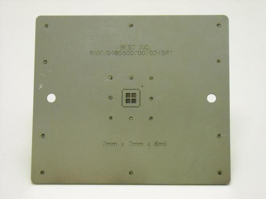
New Equipment | Solder Paste Stencils
Based on its long work on BGA rework and repair process and its in-house capability to produce metal stencils BEST can provide for you a timely, cost-effective solution for printing on to components for MOST rework systems. Our templates for printing
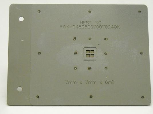
New Equipment | Solder Paste Stencils
Based on its long work on BGA rework and repair process and its in-house capability to produce metal stencils BEST can provide for you a timely, cost-effective solution for printing on to components for MOST rework systems. Our templates for printin
Electronics Forum | Wed Aug 25 15:02:04 EDT 2010 | spitkis2
I am printing solder paste directly onto a QFN device. Any recommendations on the type of solder paste to use? Namely I am concerned about getting a good release from the stencil. Thanks
Electronics Forum | Mon Dec 04 15:23:31 EST 2017 | kojotssss
A new stencil has been purchased. to be continued.
Used SMT Equipment | Screen Printers
DEK Horizon 03i automatic stencil printer Specification : DEK Horizon 03i High Precision Automatic Solder Paste Printer designed for high precision steel mesh printing or stencil printing in SMT industry. Printing PCB size: 50x50mm to 508x510mm;
Industry News | 2015-07-27 20:29:13.0
The SMTA Capital Chapter is pleased to invite you to its upcoming Capital Expo and Tech Form at Johns Hopkins Applied Physics Lab, Kossiakoff Center, 11100 Johns Hopkins Road, Laurel, MD 20723, on September 1st. Exhibitors can save $100 by taking advantage of the early registration promotion available through July 31st. Contact Kaitlyn Gherity, SMTA Expo Manager, at 952-920-7682 or kaitlyn@smta.org to exhibit.
Industry News | 2012-01-22 23:16:58.0
More than 350 engineers who attended last week’s IPC webinar, Soldering and Assembly Defects, were polled on their biggest headaches with printed boards, PCB components and PCB assembly process failures. The survey results which identify solder finish, ball grid array (BGA) components and reflow soldering as the greatest challenges, provide webinar co-sponsor, National Physical Laboratory (NPL) of the United Kingdom with useful information as it prepares its NPL Process Defect Clinic for IPC APEX EXPO® 2012.
Technical Library | 2010-09-16 18:45:06.0
With PCB complexity and density increasing and also wider use of 3D devices, tougher requirements are now imposed on device inspection both during original manufacture and at their subsequent processing onto printed circuit boards. More complicated and de
Technical Library | 2023-08-04 15:38:36.0
The MicroLeadFrame® (MLF®)/Quad Flat No-Lead (QFN) packaging solution is extremely popular in the semiconductor industry. It is used in applications ranging from consumer electronics and communications to those requiring high reliability performance, such as the automotive industry. The wide acceptance of this packaging design is primarily due to its flexible form factors, size, scalability and thermal dissipation capabilities. The adaptation and acceptance of MLF/QFN packages in automotive high reliability applications has led to the development of materials and processes that have extended its capabilities to meet the performance and quality requirements. One of process developments that is enabling the success of the MLF/QFN within the automotive industry has been the innovation of side wettable flanks that provide the capability to inspect the package lead to printed circuit board (PCB) interfaces for reliable solder joints. Traditionally, through-board X-ray was the accepted method for detecting reliable solder joints for leadless packages. However, as PBC layer counts and routing complexities have increased, this method to detect well-formed solder fillets has proven ineffective and incapable of meeting the inspection requirements. To support increased reliability and more accurate inspection of the leadless package solder joints, processes to form side-wettable flanks have been developed. These processes enable the formation of solder fillets that are detectable using state-of-the-art automated optical inspection (AOI) equipment, providing increased throughput for the surface mount technology (SMT) processes and improved quality as well.
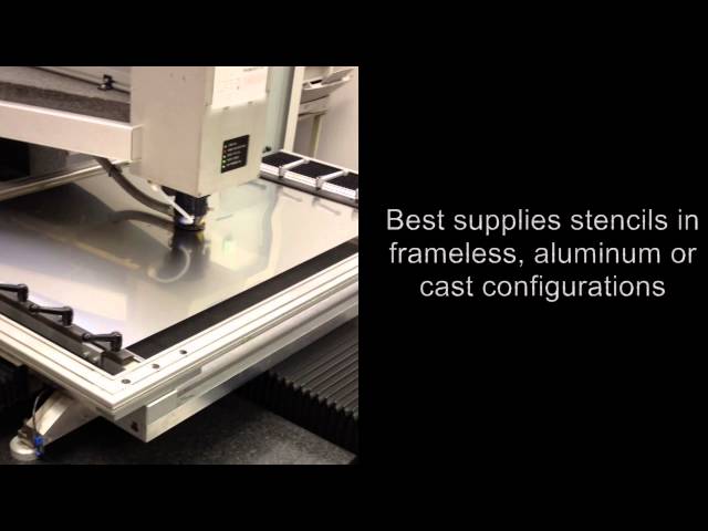
BEST manufactures and designs SMT stencils-both metal and plastic film type. This video demonstrates our metal stencil laser. See more on stencils here: http://www.soldertools.net/categories/Metal-Stencils/
BEST manufactures and designs SMT stencils-both metal and plastic film type. This video demonstrates our metal stencil laser. See more on stencils here: http://www.soldertools.net/categories/Metal-Stencils/
Training Courses | | | PCB Rework and Hand Soldering Courses
The PCB rework and hand soldering courses courses cover techniques of rework and repair of PCBs, BGAs and other electronics assemblies, and teach fundamentals of soldering of electronics assemblies.
Career Center | South Plainfield, New Jersey USA | Engineering
Alpha, a business unit of Alent plc and the global leader in the development, manufacturing and sales of innovative specialty materials used in a wide range of industry segments, including electronics assembly, power electronics, die attach, LED ligh
Career Center | , Portugal | Engineering,Maintenance,Production,Quality Control,Technical Support
SMT Process engineer Quality Efficiency Continuous improvement 11 years of experience in high volume production in a Japanese corporation Expertise in: Solder paste printing (DEK, Panasonic) Adhesive dispensing (FUJI, Panasonic) Components Pick and p
Career Center | Wesley Chapel, Florida USA | Engineering,Management,Quality Control
15 years of experience on Electronic Manufacturing. Certified SMT Process Engineer TQM Knowledge Statistics DOE Screen Printer Thermal Process Knowledge JIT International Project Engineering Experience
Minimizing Voiding In QFN Packages Using Solder Preforms SMTnet Express July 27, 2012, Subscribers: 25333, Members: Companies: 8933, Users: 33366 Minimizing Voiding In QFN Packages Using Solder Preforms First published in the 2012 IPC APEX EXPO
The Morphology Evolution and Voiding of Solder Joints on QFN Central Pads with a Ni/Au Finish SMTnet Express October 19, 2012, Subscribers: 25598, Members: Companies: 9011, Users: 33828 The Morphology Evolution and Voiding of Solder Joints on QFN
| https://ipcapexexpo.org/education/call-for-technical-paper-form
Extreme Requirements PCB Fabrication and Materials Quality, Reliability, Test and Inspection Other Assembly Processes Topics BTC/QFN/LGA Assembly Challenges Cleaning Coating Processes Electronics
| https://www.smtfactory.com/What-are-the-operating-steps-of-the-Full-auto-SMT-Stencil-Printer-id40362477.html
Series Vacuum Reflow Oven SMT Stencil Printing Machine Semi-auto SMT Stencil Printer Full-auto SMT Stencil Printer Pick & Place Machine SAMSUNG Pick


