Industry News | 2019-11-06 13:32:03.0
During the 2019 Annual Meeting at SMTA International, the SMTA honored members who have shown exceptional service to the association and the electronics assembly industry.
Industry News | 2015-03-16 06:51:04.0
Void Formation in Solder Joints – Causes & Cures Webinar Monday 18th May 2.30pm GMT Voiding in solder joints is not new we have experienced cavities in solder joints during the introduction of through hole, surface mount and more recently area array technology. In many cases we never knew we have had voids till the introduction of x-ray inspection.
Technical Library | 2022-10-31 17:25:37.0
Mixed formulation solder alloys refer to specific combinations of Sn-37Pb and SAC305 (96.5Sn–3.0Ag–0.5Cu). They present a solution for the interim period before Pb-free electronic assemblies are universally accepted. In this work, the surfaces of mixed formulation solder alloys have been studied by in situ and real-time Auger electron spectroscopy as a function of temperature as the alloys are raised above the melting point. With increasing temperature, there is a growing fraction of low-level, bulk contaminants that segregate to the alloy surfaces. In particular, the amount of surface C is nearly _50–60 at. % C at the melting point. The segregating impurities inhibit solderability by providing a blocking layer to reaction between the alloy and substrate. A similar phenomenon has been observed over a wide range of (SAC and non-SAC) alloys synthesized by a variety of techniques. That solder alloy surfaces at melting have a radically different composition from the bulk uncovers a key variable that helps to explain the wide variability in contact angles reported in previous studies of wetting and adhesion. VC 2011 American Vacuum Society. [DOI: 10.1116/1.3584821]
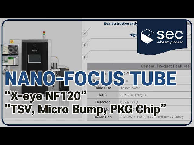
#Xray#Inspection#SEC Nano-focus Tube of 200 nano resolution which is specialized for sub-micron defects of Semiconductor Packaging, Wafer Level Packaging(WLP). -Non-destructive Analysis System -High-Resolution Image with Dual Type CTs -Application
Industry Directory | Distributor / Manufacturer
An international distributor of mechanical IC samples or "dummy" components, SMD production tools and equipment
.JPG)
Used SMT Equipment | SPI / Solder Paste Inspection
The LSM300 follows the successful Laser section Microscopes LSM and LSM2. This new non-contact laser based system is an off-Line solder paste inspection system.LSM300 provides automatic height measurements, eliminating the inconsistencies of manual m
Training Courses | | | PCB Assembly Courses
The PCB assembly courses provide knowledge of different processes and equipment used in TH and SMT assembly of printed circuit boards.
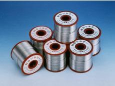
New Equipment | Solder Materials
We have a wide variety of flux-Cored solder, a mix of metal alloy, flux and other elements, that we have put together to match every type of application. This formula is designed so that the incidence of bridging is rare; likew
Industry Directory | Consultant / Service Provider / Manufacturer
Specializing in electronic circuit board assembly services. Various capabilities include engineering, assembly, designing, prototyping,supply chain management, testing, documentation, rework, repair and soldering. On-time delivery
Technical Library | 2021-07-06 21:13:36.0
The surface finishes commonly used on printed circuit boards (PCBs) have an effect on solder paste performance in the surface mount process. Some surface finishes are non-planar like hot air solder level (HASL) which can lead to inconsistencies in solder paste printing. Other surface finishes are difficult to wet during reflow like organic solderability preservative (OSP). What is the overall effect of surface finish on solder paste performance? Which solder paste is best for each surface finish? It is the goal of this paper to answer these questions.


