Industry News | 2017-04-05 11:18:26.0
Microtronic GmbH is pleased to announce that it has added the PEMTRON PS™ Series Scanning Electron Microscopes (SEMs) to its product line up in parts of the EU. The PS Series Models include the PS-210 Compact Desk Top Mini-SEM, the PS-230 High Performance Normal-SEM, and PS-250 Analytical Normal-SEM.
Industry News | 2019-05-31 08:50:57.0
Non-destructive testing of 3D packages with scanning acoustic microscopes identifies defects down to sub-micron level for 100% inspection, failure analysis
Industry News | 2019-05-31 08:56:07.0
Non-destructive testing of 3D packages with scanning acoustic microscopes identifies defects down to sub-micron level for 100% inspection, failure analysis
Industry News | 2015-04-07 15:34:16.0
Microtronic GmbH, a leading sales specialist of microelectronics, will display a range of products in Booth # 7-101L at SMT/Hybrid/Packaging, scheduled to take place May 5-7, 2015 at the Messe in Nuremberg, Germany.
Industry News | 2015-09-03 15:44:25.0
Microtronic today announced plans to exhibit at the 20th European Microelectronics and Packaging Conference & Exhibition (EMPC), scheduled to take place Sept. 14-16, 2015 in Friedrichshafen, Germany. Company representative will demonstrate the Microtronic LBT-210, Akrometrix TherMoiré AXP and Sonix ECHO™ as well as specialty solders from AIM.
Industry Directory | Consultant / Service Provider / Manufacturer
Designer & Manufacturer of Acoustic Microscopes for Nondestructive Component Inspection.
Industry Directory | Manufacturer
Designer and Manufacturer of Acoustic Microscopes for Non-destructive Ultrasonic Immersion Inspection and Semiconductor Package Failure Analysis.
Used to inspection materials which do not admit x-ray penetration (e.g. ceramics). Also used in device-level inspection for defects and counterfeit detection.
Used SMT Equipment | Semiconductor & Solar
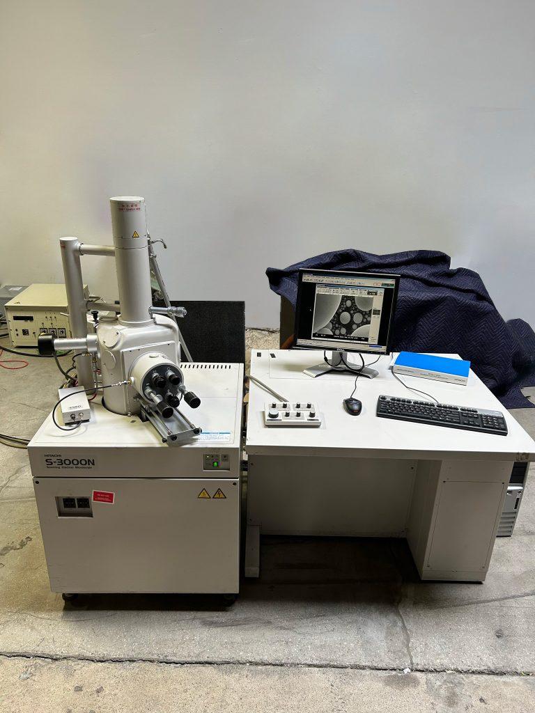
HITACHI S-3000-N Scanning Electron Microscope (SEM) Not sure of vintage! Full specifications upon request. https://www.karenmadison.com/hitachi-s-3000-n-scanning-electron-microscope-sem/
Technical Library | 2017-06-15 00:44:19.0
Ceramics packages are being used in the electronics industry to operate the devices in harsh environments. In this paper we report a study on acoustic imaging technology for nondestructively inspecting underfill layers connecting organic interposers sandwiched between two ceramics substrates.First, we inspected the samples with transmission mode of scanning acoustic tomography (SAT) system, an inspection routine usually employed in assembly lines because of its simpler interpretation criteria: flawed region blocks the acoustic wave and appears darker. In this multilayer sample, this approach does not offer the crucial information at which layer of underfill has flaws. To resolve this issue, we use C-Mode Scanning in reflection mode to image layer by layer utilizing ultrasound frequencies from 15MHz to 120MHz. Although the sample is thick and contains at least 5 internal material interfaces, we are able to identify defective underfill layer interfaces.


.png)

