Technical Library | 2017-06-15 00:44:19.0
Ceramics packages are being used in the electronics industry to operate the devices in harsh environments. In this paper we report a study on acoustic imaging technology for nondestructively inspecting underfill layers connecting organic interposers sandwiched between two ceramics substrates.First, we inspected the samples with transmission mode of scanning acoustic tomography (SAT) system, an inspection routine usually employed in assembly lines because of its simpler interpretation criteria: flawed region blocks the acoustic wave and appears darker. In this multilayer sample, this approach does not offer the crucial information at which layer of underfill has flaws. To resolve this issue, we use C-Mode Scanning in reflection mode to image layer by layer utilizing ultrasound frequencies from 15MHz to 120MHz. Although the sample is thick and contains at least 5 internal material interfaces, we are able to identify defective underfill layer interfaces.
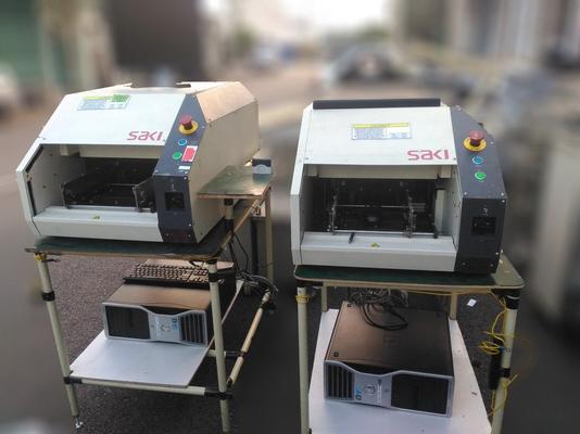
Used SMT Equipment | AOI / Automated Optical Inspection
Benchtop High Resolution, High Speed Automated Optical Inspection System Model: BF-Comet18 Resolution: 18μm Board Size: 50×50 - 250×330mm, 2×2 - 10×13in. Board Thickness: 0.6 -
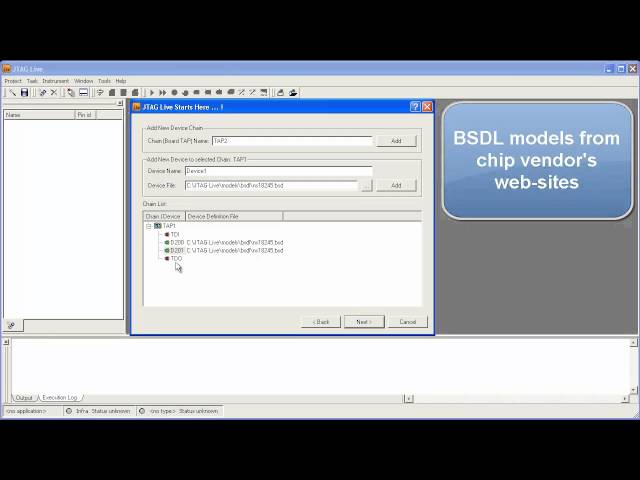
Free JTAG Live software is used for hardware debug of PCBs using boundary-scan IEEE 1149 technology. This video shows how to get to stage 1, testing the boundary-scan infrastructure. JTAG Live Buzz can be downloaded for free at http://www.jtaglive.c
Industry Directory | Manufacturer
Computrol, Inc. is a national leader in low to medium volume, high mix contract manufacturer of electronic assemblies. We specialize in customer service, quality and on time delivery. We have 3 locations in the United States.
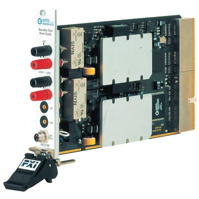
In the recent years, PXI has established its position in the test and measurement industry, especially with such features as high data transfer rates, small rugged industrial footprint, open standard and multiple vendors. PXI (PCI eXtensions for Inst

![[SEC] SEM(Scanning Electron Microscope) SNE 4500M Plus Premium Version of Highest-end](https://img.youtube.com/vi/C9ny0wTR8mY/sddefault.jpg)
#SEM#SEC#??????? Model: SNE-4500M Plus (A) / (B) Resolution: 5nm (30kV, SE Image) Magnification: 30x~150,000x Detector: Secondary Electron(SE) / Backscattered Electron(BSE) Vacuum: High / Low Stage: X,Y, Z, R, T : Fully motorized Navigation mode wi

Failure Analysis and general laboratory investigations of electronic components and devices, plus material analysis. Ideally suited for high precision scanning of high density devices.
Parts & Supplies | Soldering Equipment/Fluxes
3D Solder Paste Inspection Machine Features : Easy to use by fully motorize X-Y scan mechanism. Easy to program by Gerber image navigator Easy to repeat the same job by loading the saved program User-friendly color image live view operation Ea
Used SMT Equipment | In-Circuit Testers
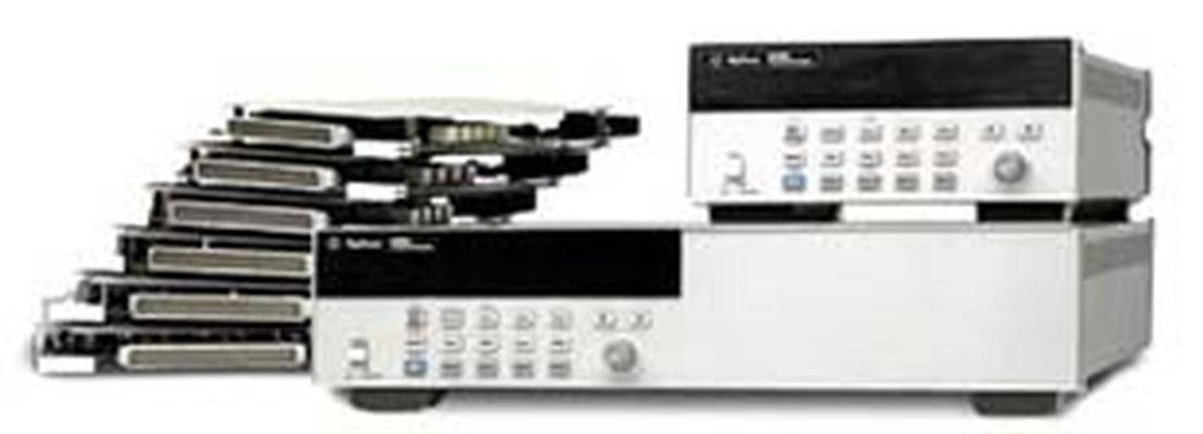
Agilent 3499A 5-Slot Switch/Control Mainframe Switch/Control Mainframe The Agilent 3499 family provides a high-speed, high-density electronic/optical switching solution for automatic test engineering (ATE) applications, with a 30% cost and sp
.jpg)


