Industry Directory | Manufacturer
Pemtron develops and manufactures 3-D Solder Paste Inspection, 3-D Nano Profilers and Scanning Electron Microscopes
Career Center | Gaithersburg, Maryland USA | Engineering,Production
Test Engineer Design hardware and software solutions required to test data communications products in a low-medium volume, high-mix production test environment. Design and build test fixtures to support these solutions. Support Production Test d
Career Center | Carleton, Michigan USA | Engineering,Sales/Marketing
Proof Of Design, a leading electronics and electromechanical engineering consultancy, needs a very knowledgeable, highly experienced test engineer to join our team for pending contracts. Must have JTAG/Boundary scan experience and the ability to trav
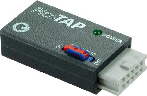
PicoTAP is the world's smallest JTAG/Boundary Scan Controller and perfect for learning Boundary Scan technology. The controller was developed to support designs of lower complexity. PicoTAP is characterised by: * small, compact and portable des
Industry Directory | Manufacturer
optical control GmbH has been involved in counting components while avoiding contact with them using X-ray technology.

The uniqueness of this JTAG/Boundary Scan Workbench has been maintained over the years through continuous integration of new, intelligent tools paired with innovative system extensions and improvements in the user interface. Today, SYSTEM CASCON™ is
We will deal with Electronic equipment and Electronics parts.
Technical Library | 2015-05-11 21:27:52.0
Originating from the last millenium, almost three decades ago, the introduction of surface mount packaging triggered a wave of changes throughout many aspects of electronics production. A small number of talented, innovative test engineers from various big players of the industry started to attend meetings to discuss the impact of that change of technology on their future test concepts for modern assemblies. The Joint Test Action Group was born.
Technical Library | 2013-08-22 14:28:58.0
Tin-rich solders are widely applied in the electronic industry in the majority of modern printed circuit boards (PCBs). Because the use of lead-tin solders has been banned in the European Union since 2006, the problem of the bridging of adjacent conductors due to tin whisker growth (limited before by the addition of Pb) has been reborn. In this study tin alloys soldered on glass-epoxy laminate (typically used for PCBs) are considered. Scanning ion microscopy with Focused Ion Beam (FIB) system and energy-dispersive X-ray spectroscopy (EDXS) were used to determine correlations between spatial non-uniformities of the glass-epoxy laminate, the distribution of intermetallic compounds and whisker growth.


