Industry Directory | Manufacturer
CSM Instruments develops, manufactures and sells instruments to characterize mechanical properties of surfaces. We have been the world leader in this market for more than 30 years.
Industry Directory | Consultant / Service Provider / Manufacturer
From the Irvine, CA office Nanovea began designing and manufacturing instruments after years of experience in providing solutions for profilometry, mechanical and tribology applications.
New Equipment | Rework & Repair Equipment
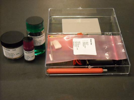
The BEST Gold Contact Replating Kit includes the tools you need for fast replating and modification of circuit contacts. Edge contacts may require replating if they are contaminated with solder or become scratched during handling or do not meet the m

New Equipment | Test Equipment
The Micro Scratch Tester is widely used to characterize adhesion failure of thin films and coatings, with a typical thickness below 5 µm. The MST is also used in the analysis of organic and inorganic; soft and hard coatings. Applications include thin
Electronics Forum | Wed Jun 24 04:18:52 EDT 2009 | satishk
We are doing SGA actibity, request please to let us know "the probables for PCB / PCBA scratches" especially in contract manufacutrers.
Electronics Forum | Sat Jun 27 08:21:13 EDT 2009 | davef
We assume you're talking about scratches of the solder mask. One possible cause is: poor handling by stacking several boards on top of another and then moving them around, most often when carrying the stack of boards from one work station to another.
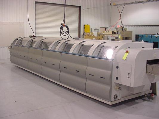
Used SMT Equipment | Board Cleaners
Details: • 20" Belt Conveyor • 10 HP Hurricane Wash & Rinse Sections • 3 Turbine Dryers (Sonic Air) (2)15HP & (
Used SMT Equipment | Pick and Place/Feeders
JUKI KE-2080E JUKI KE-2080E JUKI KE-2080E JUKI KE-2080E Y/M 2008 2011 2011 2010 operating hours 69372 63857 63421 49288 options component height 25mm 25mm 25mm 25mm Board size 510.00 x 460.00 510.00 x 460.00 510.00 x 460.00
Industry News | 2017-08-23 12:47:29.0
Count On Tools is pleased to announce that it now offers a complete line of nozzles for the Panasonic AM100 machines. These nozzle designs enable highly accurate, repeatable, optimized chip placement. The AM Series equipment maintains the high standards for capability, flexibility and reliability that customers expect in a cost-effective, incrementally scalable, high-mix SMT solution.
Industry News | 2015-02-04 17:28:59.0
Count On Tools announces that it now offers a complete line of nozzles for the Panasonic NPM machines. These nozzle designs enable highly accurate, repeatable, optimized chip placement. The NPM Series equipment optimizes the latest technologies into a lean modular solution for changing, expanding and evolving electronic assembly needs.
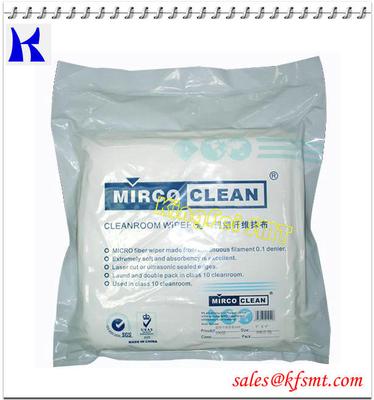
Parts & Supplies | SMT Equipment
SMT Cleanroom Microfibre Wiper paper Applications: Superior for spill control and general wiping in Class10~1,000 environments; Cleaning and polishing the products TFT-LCD, Optical and other critical industries etc.request; Maintaining critica
Parts & Supplies | Pick and Place/Feeders
Product Description: Product Name: Philips smt feeder station(with power supply) Product Size (mm): L120*W230*H250 Brand:Philips Devices Number : Install one FEEDER Applicable models: Philips Series models Weight: About 6KG This product is ma
Technical Library | 2020-08-27 01:22:45.0
Initially adopted internal specifications for acceptance of printed circuit boards (PCBs) used for wire bonding was that there were no nodules or scratches allowed on the wirebond pads when inspected under 20X magnification. The nodules and scratches were not defined by measurable dimensions and were considered to be unacceptable if there was any sign of a visual blemish on wire-bondable features. Analysis of the yield at a PCB manufacturer monitored monthly for over two years indicated that the target yield could not be achieved, and the main reasons for yield loss were due to nodules and scratches on the wirebonding pads. The PCB manufacturer attempted to eliminate nodules and scratches. First, a light-scrubbing step was added after electroless copper plating to remove any co-deposited fine particles that acted as a seed for nodules at the time of copper plating. Then, the electrolytic copper plating tank was emptied, fully cleaned, and filtered to eliminate the possibility of co-deposited particles in the electroplating process. Both actions greatly reduced the density of the nodules but did not fully eliminate them. Even though there was only one nodule on any wire-bonding pad, the board was still considered a reject. To reduce scratches on wirebonding pads, the PCB manufacturer utilized foam trays after routing the boards so that they did not make direct contact with other boards. This action significantly reduced the scratches on wire-bonding pads, even though some isolated scratches still appeared from time to time, which caused the boards to be rejected. Even with these significant improvements, the target yield remained unachievable. Another approach was then taken to consider if wire bonding could be successfully performed over nodules and scratches and if there was a dimensional threshold where wire bonding could be successful. A gold ball bonding process called either stand-off-stitch bonding (SSB) or ball-stitch-on-ball bonding (BSOB) was used to determine the effects of nodules and scratches on wire bonds. The dimension of nodules, including height, and the size of scratches, including width, were measured before wire bonding. Wire bonding was then performed directly on various sizes of nodules and scratches on the bonding pad, and the evaluation of wire bonds was conducted using wire pull tests before and after reliability testing. Based on the results of the wire-bonding evaluation, the internal specification for nodules and scratches for wirebondable PCBs was modified to allow nodules and scratches with a certain height and a width limitation compared to initially adopted internal specifications of no nodules and no scratches. Such an approach resulted in improved yield at the PCB manufacturer.
Technical Library | 2019-03-25 12:45:56.0
Work instructions are time consuming to generate for engineers, often requiring regeneration from scratch to address very minor changes. They need to be produced in varying levels of detail, with varying guidelines, for multiple stations, operators and lines. Minor component, station or process changes – down to the modification of an individual BOM component – can cause headaches when attempting to maintain consistency across multiple work instructions that are touched by the change.The solution presented here improves efficiency and saves engineering time by making use of a database driven approach. Manufacturing details, component information, process guidelines, annotations, machine-specific data, and more can be stored in one central database. Any information stored in this single repository can then be modified quickly in one location and automatically propagate seamlessly throughout multiple work instructions. These can be instantly printed out or displayed on screens at appropriately affected stations with the simple click of a button, as opposed to regenerating from scratch, or going in and reviewing many documents to find and update with the change.

Name:Semi-automatic capacitor cutting machine Model:SC-104A Voltage :220V AC 60Hz/50Hz 40W Size:L360*W300*H350MM Weight:35kg Efficiency:2500-3000PCS/H (It depends on the worker) Features: 1. suitable for bulk, tube radial parts cutting foot ope
Name:Semi-automatic capacitor cutting machine Model:SC-104A Voltage :220V AC 60Hz/50Hz 40W Size:L360*W300*H350MM Weight:35kg Efficiency:2500-3000PCS/H (It depends on the worker) Features: 1. suitable for bulk, tube radial parts cutting foot ope
Career Center | , California USA | Engineering,Management,Production
Plant Operations Manager needed to start up new division of rapidly growing EMS provider in the bay area of California. Our client is known for exceptional quality and customer satisfaction and has the awards to back them up. They actively promote
Career Center | Racine, Wisconsin USA | Engineering
Cree currently has a job vacancy for an SMT Process Technician in our Lighting Manufacturing facility in Racine, Wisconsin. Summary: This person will be a primary contributor to the startup of a new SMT production line for LED PCB Assembly. This
Career Center | Sunrise, Florida USA | Technical Support
local area field srevice technician fixing or replacing desktops and POlocal S's
Career Center | Bangalore, Karnataka India | Sales/Marketing
Dear Mam / Sir, Greetings, My 22 years of Sales & Business Development experience in “Capital Equipments” (Plastic processing m/c's, Turn-key packaging m/c’s, etc.) should be of interest to a fast growing company like yours. My experience in vario
requiring regeneration from scratch to address very
GPD Global | https://www.gpd-global.com/co_website/pdf/pbt/Wafer-Option-PBFT-SPC98-PBT-3029.pdf
. 1. Modify the Cover (Item 39) by cutting the slot and drilling the hole detailed on Drawing PBT-3012. Be careful to protect the painted surface of the cover from scratches during the modification process. 2
ASCEN Technology | https://www.ascen.ltd/Video_Channel/Non-standard_equipment/519.html
. PCB inspection machine are able to detect a variety of surface feature defects such as nodules, scratches and stains as well as the more familiar dimensional defects such as open circuits, shorts and


