Industry Directory | Distributor / Manufacturer
AllPoint Electronics is specialized in SMT, PTH, and TEST Equipment and services for electronics industry in Brazilian market. We provide full support for PCB assembly factory implementation, and process consulting
Technical Library | 2016-11-30 15:53:15.0
The use of microvias in Printed Circuit Boards (PCBs) for military hardware is increasing as technology drives us toward smaller pitches and denser circuitry. Along with the changes in technology, the industry has changed and captive manufacturing lines are few and far between. As PCBs get more complicated, the testing we perform to verify the material was manufactured to our requirements before they are used in an assembly needs to be reviewed to ensure that it is sufficient for the technology and meets industry needs to better screen for long-term reliability. The Interconnect Stress Testing (IST) protocol currently used to identify manufacturing issues in plated through holes, blind, or buried vias are not necessarily sufficient to identify problems with microvias. There is a need to review the current IST protocol to determine if it is adequate for finding bad microvias or if there is a more reliable test that will screen out manufacturing inconsistencies. The objective of this research is to analyze a large population of PCB IST coupons to determine if there is a more effective IST test to find less reliable microvias in electrically passing PCB product and to screen for manufacturing deficiencies. The proposed IST test procedure will be supported with visual inspection of corresponding microvia cross sections and Printed Wiring Assembly (PWA) acceptance test results. The proposed screening will be shown to only slightly affect PCB yield while showing a large benefit to screening before PCBs are used in an assembly.
Industry News | 2019-11-05 22:07:01.0
Tenting a via refers to covering via with soldermask to enclose or skin over the opening. A via is a hole drilled into the PCB that allows multiple layers on the PCB to be connected to each other. A non tented via is just a via that is not covered with the soldermask layer. Leaving these vias exposed or covered has pros and cons depending on the your design and manufacturing requirements.
.jpg)
Used SMT Equipment | Screen Printers
DEK Horizon 02iX Screen Printer for sale, Hawkeye Camera SKU 16533 • Hawkeye 1700 Camera • HawkEye 1700 vision window = 11.3mm x 8.7mm Dek "The most accurate results are obtained using printing machines fitted with the 1700
ISIS� (Infrared Screening and Inspection Solutions) was developed to detect defects and manufacturing flaws in printed circuit boards (PCBs) that are assembled using surface mount technology (SMT). ISIS� uses infrared imaging and proprietary thermal
Industry Directory | Consultant / Service Provider / Manufacturer
Lepla srl electronic contract manufacturer, specialized in the SMT & THT Electronic Cards Assembling, Wiring Assembling Harness, In-Circuit, Parametric and Functional Testing.
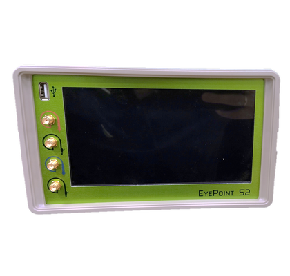
New Equipment | Test Equipment
EyePoint S2 – Desktop localizer of faulty electronic components with screen and ASA module with frequency up to 100 kHz Preview: EyePoint S2 is a simple and affordable desktop system for finding faulty electronic components on printed ci

H450 with automatic machine vision recognition function uses high-precision servo drive system to achieve fast and accuracy alignment. The precision can reach +/- 0.01mm. It has built in independent cleaning system, the cycle time less than 7s ensure
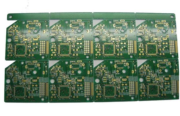
New Equipment | Fabrication Services
Low Cost Heavy Copper PCB China 4 Layers Circuit Boards Supplier Quick Details: FR4 base material 1.6mm board thickness 2oz heavy copper Plating gold finishing RF custom PCB boards Used for Radio Frequency From China PCB manufacturer Specifications


