Training Courses | | | PCB Inspection Courses
The PCB inspection courses focus on improving PCB yield and reliability through validation and detection of defects on electronics assemblies.
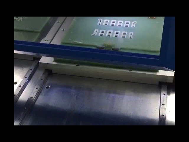
ML-2500S PCB Separator uses high speed rotation milling cutter to separate PCB array. Widely applied in digital, communication, lighting, etc. Which improved the defect on PCB separating caused by manual, V-cut, stamping, etc If you have any questi
Industry News | 2022-01-10 16:55:15.0
The SMTA Capital Chapter Officer team is excited to provide our members with a free technical webinar on "Use of Photonic Soldering to Rework Chip Components" presented by Dr. Vahid Akhavan, Global Application Engineer at NovaCentrix. The presentation will take place on January 20th at 12:00am EST.
Industry News | 2011-03-31 11:54:23.0
Over the past few years, pad cratering has become a vexing problem in lead-free assemblies, largely attributed to problems with the resin used to make a printed board. To help industry eliminate the defect and, at the same time, cut costs, IPC — Association Connecting Electronics Industries® has released IPC-9708, Test Methods for Characterization of PCB Pad Cratering.
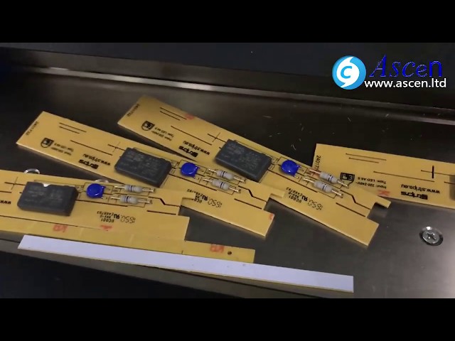
link:https://www.ascen.ltd/Blog/Solutio/493.html ASCEN PCB separator ASC-620 PCB cutting machine can use for cutting LED long board and also can use to the PCBA with the high component separate operation.It is the best way to replace the way to purch
Used SMT Equipment | Semiconductor & Solar
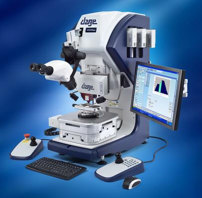
Bondtester by DAGE, in good condition. DAGE Series 4000 Bondtester product information. The 4000 bondtester is multipurpose, capable of performing all pull and shear applications. The 4000 bondtester can be configured as a simple bond wire pull
Industry News | 2017-08-02 07:12:18.0
As market leader in bond testing, XYZTEC is pushing the technology forward. In this month's newsletter we highlight the recent advances in thin, 3D and MEMS die bond testing. As developments in thin die change the shape of our customers' products, three fundamental difficulties for the bond test have to be overcome:
New Equipment | Test Equipment - Bond Testers
Nordson DAGE is the leading provider of award winning bond testing equipment. The second generation 4000Plus bondtester continues to be the most advanced bondtester on the market whilst the 4000 Optima is optimized for fast, accurate and reliable bon
Technical Library | 2015-08-13 15:52:40.0
Pad cratering has become more prevalent with the switch to lead free solders and lead free compatible laminates. This mainly is due to the use of higher reflow temperature, stiffer Pb-free solder alloys, and the more brittle Pb-free compatible laminates. However, pad cratering is difficult to detect by monitoring electric resistance since pad cratering initiates before an electrical failure occurs. Several methods have been developed to evaluate laminate materials' resistance to pad cratering. Pad-solder level tests include ball shear, ball pull and pin pull. The detailed methods for ball shear, ball pull, and pin pull testing are documented in an industry standard IPC-9708. Bansal, et al. proposed to use acoustic emission (AE) sensors to detect pad cratering during four-point bend test. Currently there is an industry-working group working on test guidelines for acoustic emission measurement during mechanical testing.
Technical Library | 2021-11-03 17:05:39.0
Additively printed circuits provide advantages in reduced waste, rapid prototyping, and versatile flexible substrate choices relative to conventional circuit printing. Copper (Cu) based inks along with intense pulsed light (IPL) sintering can be used in additive circuit printing. However, IPL sintered Cu typically suffer from poor solderability due to high roughness and porosity. To address this, hybrid Cu ink which consists of Cu precursor/nanoparticle was formulated to seed Cu species and fill voids in the sintered structure. Nickel (Ni) electroplating was utilized to further improve surface solderability. Simulations were performed at various electroplating conditions and Cu cathode surface roughness using the multi-physics finite element method. By utilizing a mask during IPL sintering, conductivity was induced in exposed regions; this was utilized to achieve selective Ni-electroplating. Surface morphology and cross section analysis of the electrodes were observed through scanning electron microscopy and a 3D optical profilometer. Energy dispersive X-ray spectroscopy analysis was conducted to investigate changes in surface compositions. ASTM D3359 adhesion testing was performed to examine the adhesion between the electrode and substrate. Solder-electrode shear tests were investigated with a tensile tester to observe the shear strength between solder and electrodes. By utilizing Cu precursors and novel multifaceted approach of IPL sintering, a robust and solderable Ni electroplated conductive Cu printed electrode was achieved.


