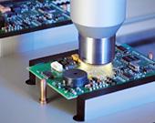
PLASMATREAT: Openair Plasma Process, Eliminating all Organic and Silicon-Based Contaminants Effectively Removes Electrostatically Attached Dust Applicable to Flat Surfaces as well as Complex 3D Shapes Atmospheric Plasma Process Reduces O
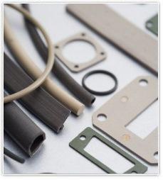
Our conductive silicone gaskets are constructed from silicone containing metal powder fillers which combine to produce high levels of attenuation with excellent environmental shielding and a high level of conductivity. Many types of filler, from nick
Electronics Forum | Tue May 27 11:59:14 EDT 2003 | blnorman
Is anyone aware of any reports, studies, articles on the subject of silicon contamination in SnPb solder joints. We are evaluating repair of conformally coated (silicone) boards. The fear is that we will never totally remove the silicone and once i
Electronics Forum | Wed May 28 11:56:18 EDT 2003 | blnorman
Yes we are using "silicones", but to find this contaminant we were looking for "silicon" the element by SEM/EDS. We use Dow materials and my contact there is checking to see if they have any info.
Industry News | 2012-10-18 19:02:31.0
IPC and SMTA jointly announce the agenda for Session 2 of the High-Reliability Cleaning and Coating Conference, scheduled to take place November 13-15, 2012 at the Crowne Plaza Hotel
Industry News | 2018-05-30 16:32:42.0
ACL introduces two new lint-free wipe materials for critical cleaning to its Contamination Control line for applications which require pristine surfaces and extrinsic contamination removal.
Technical Library | 2013-02-07 17:01:46.0
Silicone contamination is known to have a negative impact on assembly processes such as soldering, adhesive bonding, coating, and wire bonding. In particular, silicone is known to cause de-wetting of materials from surfaces and can result in adhesive failures. There are many sources for silicone contamination with common sources being mold releases or lubricants on manufacturing tools, offgassing during cure of silicone paste adhesives, and residue from pressure sensitive tape. This effort addresses silicone contamination by quantifying adhesive effects under known silicone contaminations. The first step in this effort identified an FT-IR spectroscopic detection limit for surface silicone utilizing the area under the 1263 cm-1 (Si-CH3) absorbance peak as a function of concentration (µg/cm2). The next step was to pre-contaminate surfaces with known concentrations of silicone oil and assess the effects on surface wetting and adhesion. This information will be used to establish guidelines for silicone contamination in different manufacturing areas within Harris Corporation... First published in the 2012 IPC APEX EXPO technical conference proceedings.
Technical Library | 1999-08-05 10:45:36.0
In 1998, the International 300 mm Initiative (I300I) demonstration and characterization programs will focus on 180 nm technology capability. To support these activities, I300I and equipment supplier demonstration partners must use starting silicon wafers with key parameters specified at a level appropriate level for 180 nm processing, including contamination and lithographic patterning. This document describes I300I's silicon wafer specifications, as developed with the I300I Silicon Working Group (member company technical advisors) and SEMI Standards.

A brief demonstration of the ScanCAD Precision Material Removal System for PCB Reverse Engineering

Conformal Coating Removal: Micro Abrasive Blasting helps remove conformal coating with precision avoiding any damage to the target circuit boards. This is so useful in semiconductor, electronics and medical industries. It's cost-effective. It's envi
Events Calendar | Wed Dec 04 00:00:00 EST 2019 - Wed Dec 04 00:00:00 EST 2019 | San Jose, California USA
SMTA Silicon Valley Expo & Tech Forum
Events Calendar | Tue Dec 08 00:00:00 EST 2020 - Tue Dec 08 00:00:00 EST 2020 | Online,
SMTA California Technology Day
SMTnet Express February 7, 2013, Subscribers: 26168, Members: Companies: 13281, Users: 34286 Effect of Silicone Contamination on Assembly Processes Silicone contamination is known to have a negative impact on assembly processes such as soldering
ASCEN Technology | https://www.ascen.ltd/Blog/Solutio/598.html
) Very good abrasion resistance Silicon: Silicon conformal coating PCB are most preferred in high temperature environments due to their ability to withstand high temperatures and high vibrations
| https://www.eptac.com/faqs/ask-helena-leo/ask/gold-wire-bond-failing-pull-test
. For beam lead devices: (d-1) Silicon broken. (d-2) Beam lifting on silicon. (d-3) Beam broken at bond. (d-4) Beam broken at edge of silicon. (d-5


winsouce.jpg)
