Optical polishing, edge polishing, dicing, flat lapping and machining of all hard materials including ceramic substrates, quartz, AlN, glass and sapphire windows, silicon wafers and very thin substrates and windows.
Supplying full range of the wafer shipper from 150mm to 300mm for both silicon wafer and solar wafer; wafer's foam and wafer's separator
We produce 2�, 3�, 4�, 5� and 6� silicon ingots and wafers Boron, Phosphorus, Arsenic and Antimony doped for Microelectronics and 4�, 5�, 6� and 6,5� round and pseudosquare ingots for Solar application.
Technical Library | 2009-09-09 15:08:19.0
Stencil printing equipment has traditionally been used in the surface mount assembly industry for solder paste printing. In recent years the flexibility of the tool has been exploited for a wide range of materials and processes to aid semiconductor packaging and assembly. One such application has been the deposition of adhesive coatings onto the backside of silicon wafers.
Industry Directory | Manufacturer
Porous ceramic vacuum chuck table or Polishing Chuck table supplied to semiconductor industry for silicon wafer dicing or finishing purposes. This product is an uniform compact frame, high strength, g
wafer-handling and chamber components
Industry Directory | Manufacturer
Mitel Corporation (NYSE:MLT)(TSE:MLT) is a designer, manufacturer and marketer of semiconductors, su
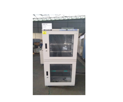
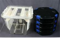
Used SMT Equipment | Drying Equipment
BRAND : SUPER DRY -02 SERIES MODEL : SD-3032-02 DESCRIPTIONS : "02 series are equipped with 1 patented dry unit to constantly main
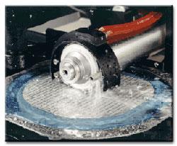
Our fully automated silicon wafer dicing service consistently meet the tight requirements expected in our industry and demanded by our customers. At Syagrus Systems, we know that a good wafer dicing or wafer cutting process sets the pace for all rema
Industry Directory | Distributor
3T Frontiers is a industrial supplier for the electronics/ semiconductor / general manufacturing industries. Our products include Epoxy adhesives, ACF (Anisotropic Conductive Film), Silicone Rubber, ND-Filters, semiconductor wafer


