Technical Library | 2021-09-21 20:20:22.0
The electronics industry has been using the epoxy puck for the processing of the vast majority of electronics microsections since the 1970s. Minimal advancements have been seen in the methods used for precision micro-sections of PCBs, PCBAs, and device packages. This paper will discuss different techniques and approaches in performing precision and analytical micro-sections, which fuse the techniques and materials common in preparation of silicon wafers and bulk materials. These techniques have not only been found to produce excellent optical results, but transfer effectively to SEM for high magnification inspection and further analysis with minimal post-lapping preparation needed. Additionally, processing time is reduced primarily due to a significant reduction of bulk material removal earlier in the preparation, therefore needing less removal at later lapping steps compared to traditional sectioning methods. Additional techniques are introduced that mitigate some classic challenges experienced by technicians over the decades.
Technical Library | 2020-01-15 23:54:34.0
Flexible electronics has significantly advanced over the last few years, as devices and circuits from nanoscale structures to printed thin films have started to appear. Simultaneously, the demand for high-performance electronics has also increased because flexible and compact integrated circuits are needed to obtain fully flexible electronic systems. It is challenging to obtain flexible and compact integrated circuits as the silicon based CMOS electronics, which is currently the industry standard for high-performance, is planar and the brittle nature of silicon makes bendability difficult. For this reason, the ultra-thin chips from silicon is gaining interest. This review provides an in-depth analysis of various approaches for obtaining ultra-thin chips from rigid silicon wafer. The comprehensive study presented here includes analysis of ultra-thin chips properties such as the electrical, thermal, optical and mechanical properties, stress modelling, and packaging techniques. The underpinning advances in areas such as sensing, computing, data storage, and energy have been discussed along with several emerging applications (e.g., wearable systems, m-Health, smart cities and Internet of Things etc.) they will enable. This paper is targeted to the readers working in the field of integrated circuits on thin and bendable silicon; but it can be of broad interest to everyone working in the field of flexible electronics.
Career Center | Charlton, Massachusetts USA | Engineering,Management,Production,Research and Development
MANUFACTURING / PROCESS ENGINEER Fused Fiber Optics company is seeking a Process Engineer to support its Optical Fabrication department. This position will be responsible for process development, optimization and troubleshooting, as well as the prep

This is the first in a series of 10-minute videos to introduce new users to the basics of machine vision technology. In this video, users will learn what machine vision is, how it is used in factory automation, and its four most common applications.
Industry News | 2018-12-08 03:20:37.0
Top Silicon Wafer Manufacturing Companies in the World
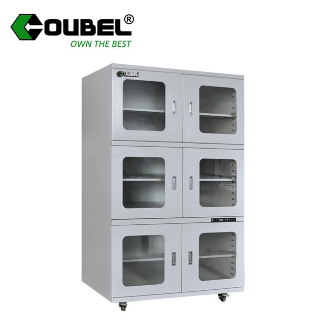
New Equipment | Board Handling - Storage
Features: 1.The humidity value is controlled between 1% and 50% RH. 2.Environmental protection and energy saving, using physical molecular sieve dehumidification method, can be reused repeatedly, dehumidification effect is good, and low power consu
Fill in the RFQ at our website for Fast Free Quotation: https://allwin21.com/semiconductor-process-equipment/rfq-rapid-thermal-processing-system/ Type: The most popular , production proven model of Desktop, Atmospheric, Manual Load/Unload RTP RTA R
Industry News | 2002-02-22 07:36:58.0
Taiwan Semiconductor Manufacturing Company (TSMC) will join Dutch Philips Electronics NV and Franco-Italian STMicroelectronics in a project to develop production lines for 300mm silicon wafers for semiconductors, an industry source told Reuters on Thursday.
STATS ChipPAC is a leading provider of advanced semiconductor packaging and test services to global customers in the communication, consumer and computing markets.
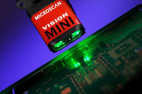
Machine vision uses image capture and analysis to automate tasks such as inspection, gauging, and counting, in addition to reading barcodes and optical characters (OCR). While human inspectors can visually inspect parts to judge the quality of workma


.png)

