Industry Directory | Consultant / Service Provider / Manufacturer
One-stop PCBs service : Design, Manufacturing, Assembly:Low Price, Express, Quality More than 1000 electronic professionals using our services. 4 layers prototype cost up from USD 50.
Industry Directory | Distributor / Manufacturer
Top 20 High-Quality PCB Fabrication and one-stop Turnkey PCB Assembly Facilities worldwide. Served national engineers for over 15 years, becoming a household name in providing full-feature multilayer PCBs engineers can trust.

New Equipment | Assembly Services
The board is designed by customer and it's for Air Purification control PCBA board. We did one-Stop EMS Service for this project (PCB manufacture, components sourcing, SMT and THT assembly): Product name: 2 Layer PCBA board Material: FR-4 Thicknss:
New Equipment | Assembly Services
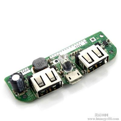
The board is designed by customer and it's for Power Bank PCBA board. We did one-Stop EMS Service for this project (PCB manufacture, components sourcing, SMT and THT assembly): Product name: 2 Layer PCBA board Material: FR-4 Thicknss: 1.6mm Surface:
Electronics Forum | Wed Feb 20 10:26:56 EST 2013 | wbailey
I am getting a lot of false calls on our AOI(YTV F1)on low contrast part markings like brown-on-yellow tantalum capacitors and etched oscillators, and on lead banks where the pcb has the part outlined in silkscreen. We are contract and cannot change
Electronics Forum | Wed Feb 20 18:04:56 EST 2013 | hegemon
You should have a number of lighting options to deal with the low contrast lettering. Low angle, B/W, reverse color. etc... If I am reading you right, you might have your bridge inspector too far out on the lead banks, that it is seeing the silkscree
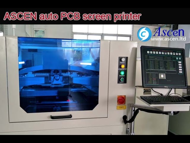
https://www.ascen.ltd/Products/Solder_paste_printer/513.html full auto PCB screen printer and SMT solder paste printing machine with Image and optical system,It is a very accurate fully automatic SMT stencil printer.automatic PCB screen printer main
Imagineering, Inc. | https://www.pcbnet.com/blog/how-pcbs-are-made/
: Copper is used to create conductive pathways on the PCB. Solder Mask: This is a protective layer, typically made of epoxy resin. It’s applied to certain board areas to protect them from the soldering process. Silkscreen
PCB Libraries, Inc. | https://www.pcblibraries.com/forum/RSS_sod882d-package-dual-flat-with-lead_topic2477.xml
;Library Expert auto-generates the drafting outlines for silkscreen Legend, Assembly, Courtyard Excess, Package Body and Terminal Lead and it adds the Pin 1 polarity marking and the proper reference designators.


