
Industry Directory | Consultant / Service Provider / Media / Publisher / Online Resource / Other
PCB Libraries' "Footprint Expert" suite uses CAD LEAP(tm) Technology to greatly simplify footprint and 3D STEP model creation; it is used by tens of thousands of PCB designers and engineers all over the world.
Industry Directory | Consultant / Service Provider / Manufacturer
Our 100% hungarian owned company is focusing on manufacturing, developing and merchandising novel products using LED technology.

We are well versed in the following thermal application materials: Sil-Pad thermally conductive insulators Gap-Pad thermally conductive gap filling material Q-Pad thermal grease replacement film Bond-Ply thermally conductive adh
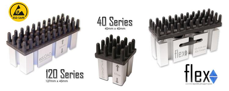
New Equipment | Board Handling - Pallets,Carriers,Fixtures
Count On Tools Inc., a leading provider of precision components and SMT spare parts, introduces the new ezLOAD PCB Support System. With the recent increase of densely populated double-sided circuit boards, COT recognized the need for more affordable
Electronics Forum | Fri Nov 09 10:15:27 EST 2007 | devajj
Of course if you are an OEM you could go back to your design engineers and tell them via's in SMD pads is unacceptable. Put that in your DFM design guidelines. If you are an EMS provider you can also influence your customer by explaining the impa
Electronics Forum | Mon Nov 30 08:39:05 EST 2015 | spoiltforchoice
http://blog.screamingcircuits.com/2010/09/smd-vs-nsmd.html such as this? Which handily also tells you what you might want to google.
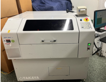
Used SMT Equipment | In-Circuit Testers
Description Make: Takaya Model: APT-9411CE Year: 2010 Type: Flying Probe Details: Takaya APT 9411 CE Flying Probe The APT-9411CE is designed for users who are looking for a precise and reliable test system with an easy to use softwar
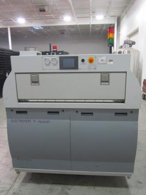
Used SMT Equipment | Board Cleaners
Speedline Technologies AquaJet Stencil Batch Cleaner and Resys ClosedLoop System For Sale The wash needs a control board. (Part Description: BL1700 CNTRL 16IN 16OUT) The Part Number to Purchase this board is 20-101-0214. Estimated cost is $349. We h
Industry News | 2003-03-18 10:12:41.0
The Falcom JP7 is a single-board GPS receiver with 12 parallel channels.
Industry News | 2003-06-17 08:07:40.0
The Radiall SMT coupler range now includes the new 14.2 x 5.1mm mini type.
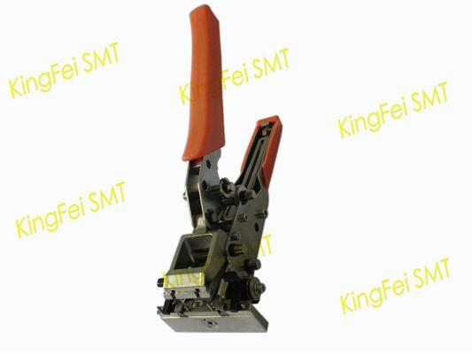
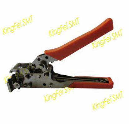
Parts & Supplies | Assembly Accessories
Features: smt splice tool 1) Designed specifically for SMD carrier tapes from 8mm to 44mm 2) Cutting tool is specially designed for precise cutting of SMD carrier tapes prior to splicing. 3) The Splice tool joins together all sizes of SMD carrier
Parts & Supplies | Assembly Accessories
Features: smt splice tool 1) Designed specifically for SMD carrier tapes from 8mm to 44mm 2) Cutting tool is specially designed for precise cutting of SMD carrier tapes prior to splicing. 3) The Splice tool joins together all sizes of SMD carrier
Technical Library | 2020-04-14 15:49:38.0
The number of through-hole components on printed circuit boards (PCB) has declined significantly over the last decade. Miniaturization in electronics has resulted in less THT (through-hole technology) and leads with a finer pitch. For this reason, the soldering of these components has also changed from wave soldering to Point-to-point selective soldering. Soldering these small, fine-pitch components is a challenge when surface mount components (SMD) are positioned very close to THT components on the PCB layout. This study, done in cooperation with a large automotive EMS customer, defines the process windows for through-hole technology for fine-pitch components. It determines what is feasible to solder and defines layout design parameter that make soldering possible with SMD areas and other components on the assembly.
Technical Library | 2020-05-08 18:22:31.0
A customer contacted the Helpline to perform analysis on a lead-free assembly which exhibited intermittent functionality. The lead-free assembly exhibiting intermittent functionality when pressure was applied to the ball grid array (BGA) packages. Industrial adaptation of a Restriction of Hazardous Substances (RoHS) compliant solder standard has created a new host of failure modes observed in lead-free assemblies. Pad cratering occurs when fractures propagate along the epoxy resin layer on the underside of the BGA connecting pads. While originating from process, design, and end use conditions, it is the combination of a rigid lead-free solder with inflexible printed circuit board (PCB) laminates that has advanced the prevalence of this condition. Pad cratering is simply the result of mechanical stress exceeding material limitations.

www.unisoft-cim.com/pcbtest.htm - In minutes the Unisoft ProntoTEST-FIXTURE software translates CAD & BOM files into real reference designators, netlists, X/Y component pin geometries, values, tolerances, part numbers, etc. This data is used by Test

Factory price automatic bare board loaders vacuum pcb loader for smt line APPLICATION The Bare Board Loader is used for automatically loading unpopulated boards at the beginning, or in the middle of a PCB assembly line. The bare boards are l
Training Courses | | | PCB Rework and Hand Soldering Courses
The PCB rework and hand soldering courses courses cover techniques of rework and repair of PCBs, BGAs and other electronics assemblies, and teach fundamentals of soldering of electronics assemblies.
Training Courses | | | PCB Rework and Hand Soldering Courses
The PCB rework and hand soldering courses courses cover techniques of rework and repair of PCBs, BGAs and other electronics assemblies, and teach fundamentals of soldering of electronics assemblies.
Events Calendar | Thu Oct 03 00:00:00 EDT 2019 - Thu Oct 03 00:00:00 EDT 2019 | ,
IPC Tech Ed Webinar Series: Ball Grid Array (BGA) and Bottom Termination Component (BTC) Design and Assembly Challenges: Reflow Profiling to Achieve Low Defect Rates and Successful Assembly! – Part 2
Events Calendar | Wed Apr 20 00:00:00 EDT 2022 - Wed Apr 20 00:00:00 EDT 2022 | ,
Virtual Course: Selection Criteria of Surface Finish for Next Generation PCB Technologies
Career Center | Marietta, Georgia USA | Engineering,Production
Currently seeking a senior pcb designer with Veribest cad experience. Knowledge of RF circuit design parameters, high density, multi-layer, and double sided. Analog/digital smd circuit board strongly desired. Designer will be responsible for pcb boar
Career Center | Fort Worth, Texas USA | Production
The requirements for the Manufacturing Engineer are a BS in Engineering with surface mount device(SMD),surface mount technology (SMT) thru-hole, and wave solder knowledge. Also, experience in fixture design, developing manufacturing processes and rel
Career Center | Bangalore, India | Engineering,Maintenance,Production,Technical Support
SMT Stencil designing & Knowledge of full SMT process software known CAD/CAM -circuit CAM Pro 7.3,GC Power station, GCCAM Edit,Auto CAD, Fault finding of Electronic Boards & Servicing electronic machines.
PCB Libraries, Inc. | https://www.pcblibraries.com/forum/ipc7351-and-smd-pad-shapes_topic2590.html
IPC-7351 and SMD Pad Shapes - PCB Libraries Forum Forum Home > Libraries > Footprints / Land Patterns New Posts FAQ Search Events Register Login IPC-7351 and SMD Pad Shapes
ASYMTEK Products | Nordson Electronics Solutions | https://www.nordson.com/en/divisions/dage/application/smd-shear
Shear testing is the main test performed for SMD due to component design issues. For example, leadless devices cannot be pull tested as there are no leads to pull upwards and as such must be shear tested to prove their effectiveness


