Technical Library | 2023-01-17 17:27:13.0
Reflow profile has significant impact on solder joint performance because it influences wetting and microstructure of the solder joint. The degree of wetting, the microstructure (in particular the intermetallic layer), and the inherent strength of the solder all factor into the reliability of the solder joint. This paper presents experimental results on the effect of reflow profile on both 63%Sn 37%Pb (SnPb) and 96.5%Sn 3.0%Ag 0.5%Cu (SAC 305) solder joint shear force. Specifically, the effect of the reflow peak temperature and time above solder liquidus temperature are studied. Nine reflow profiles for SAC 305 and nine reflow profiles for SnPb have been developed with three levels of peak temperature (230 o C, 240 o C, and 250 o C for SAC 305; and 195 o C, 205 o C, and 215 o C for SnPb) and three levels of time above solder liquidus temperature (30 sec., 60 sec., and 90 sec.). The shear force data of four different sizes of chip resistors (1206, 0805, 0603, and 0402) are compared across the different profiles. The shear force of the resistors is measured at time 0 (right after assembly). The fracture surfaces have been studied using a scanning electron microscopy (SEM) with energy dispersive spectroscopy (EDS)
Technical Library | 2023-01-17 17:22:28.0
The impact of voiding on the solder joint integrity of ball grid arrays (BGAs)/chip scale packages (CSPs) can be a topic of lengthy and energetic discussion. Detailed industry investigations have shown that voids have little effect on solder joint integrity unless they fall into specific location/geometry configurations. These investigations have focused on thermal cycle testing at 0°C-100°C, which is typically used to evaluate commercial electronic products. This paper documents an investigation to determine the impact of voids in BGA and CSP components using thermal cycle testing (-55°C to +125°C) in accordance with the IPC- 9701 specification for tin/lead solder alloys. This temperature range is more typical of military and other high performance product use environments. A proposed BGA void requirement revision for the IPC-JSTD-001 specification will be extracted from the results analysis.
Industry News | 2003-01-27 10:27:31.0
At a New Facility Within the Company's U.S. Headquarters
Industry News | 2005-09-19 16:07:56.0
No higher temperature and No process changes needed
Industry News | 2003-02-17 08:40:25.0
To Meet Government Environmental Standards and Individual Company Policies, While Satisfying Production Requirements
Industry News | 2003-06-10 08:16:44.0
The following text describes the application of NWA Quality Analyst to quality control in the assembly of electronic components.
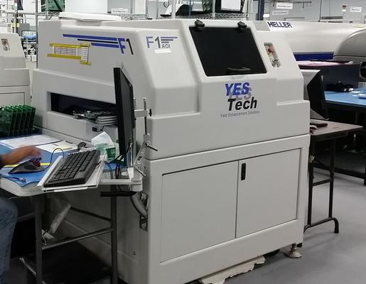
Used SMT Equipment | AOI / Automated Optical Inspection
YesTech YTV-F1 Automated PCB Inspection System >Multi-function all purpose In-Line system • (2) Top-down Cameras; Incl. (1) High Magnification • (4) side viewing cameras • LED top light, bi-color multiangle LED lighting •

Used SMT Equipment | AOI / Automated Optical Inspection
YesTech YTV-F1 Automated PCB Inspection System >Multi-function all purpose In-Line system • (2) Top-down Cameras; Incl. (1) High Magnification • (4) side viewing cameras • LED top light, bi-color multiangle LED lighting •
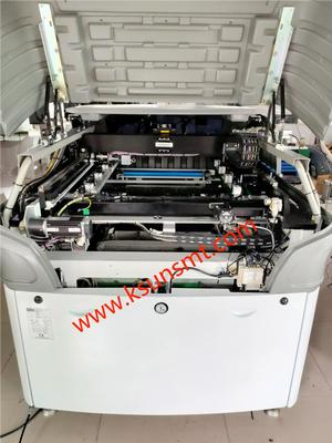
Used SMT Equipment | Screen Printers
DEK Horizon 03i automatic stencil printer Specification : DEK Horizon 03i High Precision Automatic Solder Paste Printer designed for high precision steel mesh printing or stencil printing in SMT industry. Printing PCB size: 50x50mm to 508x510mm;
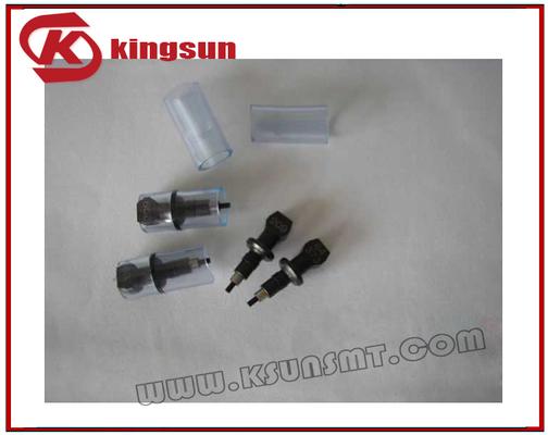
Parts & Supplies | SMT Equipment
Yamaha YG100B nozzle YAMAHA nozzle in stock YAMAHA YV100II 31#NOZZLE 0402 / 0603 / 0805 (X) YAMAHA YV100II 32#NOZZLE For IC of tiny size YAMAHA YV100II 39#NOZZLE 0603 "O" hole YAMAHA YV100II 33#NOZZLE For IC YAMAHA YV100II 34#NOZZLE For IC YA
winsouce.jpg)
.gif)

