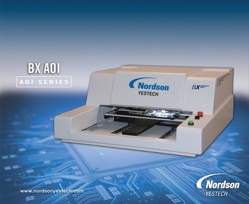
500,000 components per hour Maximum Board Size: 18” x 20” (457mm x 508mm) Clearance: 2” (50mm) top and bottom Minimum Component Size: 0201; 01005 with high magnification option
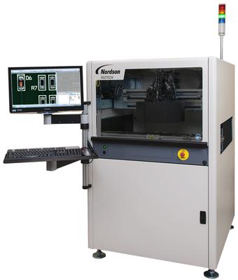
1.5 million components per hour Maximum Board Size: 20” x 21” (500mm x 525mm) Clearance: 2” (50mm) top and bottom Minimum Component Size: 0201; 01005 with high magnification option
Industry News | 2011-01-12 15:27:11.0
Ironwood Electronics recently introduced a new BGA socket addressing high performance requirements for testing digital camera processor - CBT-BGA-7005. The contactor is a stamped spring pin with 26 gram actuation force per ball and cycle life of 500,000 insertions.

Used SMT Equipment | AOI / Automated Optical Inspection
R Front Rail Fixed Application Version: 7.20C (RNS) Ladder Version: 7.100B (RNS) Image Resolution: 15um AC 120V, 2 Phase, 50/60 Hz, 1.5 kVA Max Current: 15A Hardware Configuration: Image Signal Input Unit: - Camera: 3-CCD Camera - Illumi
Parts & Supplies | Repair/Rework
main features The full-automatic BGA Ball Mounting machine PG-FA6800 is composed of IPC control system, high-speed 12 axis motion control system, high definition Vision inspection system, convenient operation system, and automatic orientation contr

Parts & Supplies | Repair/Rework
main features The full-automatic BGA Ball Mounting machine PG-FA6800 is composed of IPC control system, high-speed 12 axis motion control system, high definition Vision inspection system, convenient operation system, and automatic orientation contr
Technical Library | 2015-08-13 15:52:40.0
Pad cratering has become more prevalent with the switch to lead free solders and lead free compatible laminates. This mainly is due to the use of higher reflow temperature, stiffer Pb-free solder alloys, and the more brittle Pb-free compatible laminates. However, pad cratering is difficult to detect by monitoring electric resistance since pad cratering initiates before an electrical failure occurs. Several methods have been developed to evaluate laminate materials' resistance to pad cratering. Pad-solder level tests include ball shear, ball pull and pin pull. The detailed methods for ball shear, ball pull, and pin pull testing are documented in an industry standard IPC-9708. Bansal, et al. proposed to use acoustic emission (AE) sensors to detect pad cratering during four-point bend test. Currently there is an industry-working group working on test guidelines for acoustic emission measurement during mechanical testing.
Technical Library | 2009-11-05 11:17:32.0
Head-in-pillow (HiP), also known as ball-and-socket, is a solder joint defect where the solder paste deposit wets the pad, but does not fully wet the ball. This results in a solder joint with enough of a connection to have electrical integrity, but lacking sufficient mechanical strength. Due to the lack of solder joint strength, these components may fail with very little mechanical or thermal stress. This potentially costly defect is not usually detected in functional testing, and only shows up as a failure in the field after the assembly has been exposed to some physical or thermal stress.
Industry Directory | Consultant / Service Provider
Serving the Educational Needs of Modern Technologies
Technical Library | 2022-12-19 18:59:51.0
Material and Process Characterization studies can be used to quantify the harmful effects that might arise from solder flux and other process residues left on external surfaces after soldering. Residues present on an electronic assembly can cause unwanted electrochemical reactions leading to intermittent performance and total failure. Components with terminations that extend underneath the package can trap flux residue. These bottom terminated components are flush with the bottom of the device and can have small solderable terminations located along the perimeter sides of the package. The clearance between power and ground render high electrical forces, which can propagate electrochemical interactions when exposed to atmospheric moisture (harsh environments). The purpose of this research is to predict and understand the functional performance of residues present under single row QFN component packages. The objective of the research study is to develop and collect a set of guidelines for understanding the relationship between ionic contamination and electrical performance of a BTC component when exposed to atmospheric moisture and the trade-offs between electrical, ionic contamination levels, and cleanliness. Utilizing the knowledge gained from undertaking the testing of QFN components and associated DOE, the team will establish a reference Test Suite and Test Spec for cleanliness.


.png)