Technical Library | 2013-07-25 14:02:15.0
Bottom-termination components (BTC), such as QFNs, are becoming more common in PCB assemblies. These components are characterized by hidden solder joints. How are defects on hidden DFN joints detected? Certainly, insufficient solder joints on BTCs cannot be detected by manual visual inspection. Nor can this type of defect be detected by automated optical inspection; the joint is hidden by the component body. Defects such as insufficients are often referred to as "marginal" defects because there is likely enough solder present to make contact between the termination on the bottom-side of the component and the board pad for the component to pass in-circuit and functional test. Should the board be subjected to shock or vibration, however, there is a good chance this solder connection will fracture, leading to an open connection.
Industry Directory | Manufacturer
Kewei Tin Industry Company, established in 2006, located in Shenzhen mainly focus on Solder Products R&D, provide solder wire/solder bar/solder paste/tin anode/tin balls/soldering flux etc...
Industry News | 2017-09-03 08:06:25.0
Our latest Process Defect Photo Guide entitled “Guide to QFN/LGA & BTC Process Defects” will be released on 16th October. This optical and x-ray guide covers the most common components, assembly process and reliability failures that may occur using these parts
Technical Library | 2015-06-11 21:20:29.0
The use of bottom terminated components (BTC) has become widespread, specifically the use of Quad Flat No-lead (QFN) packages. The small outline and low height of this package type, improved electrical and thermal performance relative to older packaging technology, and low cost make the QFN/BTC attractive for many applications.Over the past 15 years, the implementation of the QFN/BTC package has garnered a great amount of attention due to the assembly and inspection process challenges associated with the package. The difference in solder application parameters between the center pad and the perimeter pads complicates stencil design, and must be given special attention to balance the dissimilar requirements
We Offer: Robotic and semi-automatic hot solder dipping, Precision lead forming of critical devices, Tape-and-reel packaging, State-of-the-art Ball Grid Array (BGA) reflow process
Industry Directory | Manufacturer
We manufacture and market stencil rolls for the PCBA industry. The cleaning material is ideal for cleaning stencils with fine pitch apertures. It prevents smearing, solder balls and other problems on the PC boards. Our stencil product is of high g
Industry Directory | Manufacturer
We are manufacturer of key products for semiconductor back end process and interconnect materials. Our main products:solder balls, Bonding wire (Au, Ag, Cu, Pd-Cu),sputtering target & EVM materials.
Industry News | 2018-11-27 11:48:56.0
Indium Corporation earned the Mexico Technology Award for its Indium10.1HF Solder Paste. The Mexico Technology Awards, sponsored by Mexico EMS, recognizes the best electronics manufacturing innovations in the electronics manufacturing industry in Mexico produced by OEM manufacturing equipment and materials suppliers over the last year.
Technical Library | 2016-11-30 21:30:50.0
Mid-chip solder balling is a defect typically associated with solder paste exhibiting poor hot slump and/or insufficient wetting during the reflow soldering process, resulting in paste flowing under the component or onto the solder resist. Once molten, this solder is compressed and forced to the side of the component, causing mid-chip solder balling.This paper documents the experimental work performed to further understand the impact on mid-chip solder balling from both the manufacturing process and the flux chemistry.
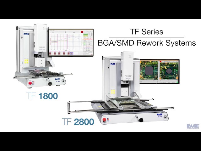
Enter PACE’s TF Series BGA/SMD Rework Systems. With its groundbreaking, patented Inductive-Convection Heating Technology, the TF Series top-side heater reaches the target temperature in just seconds for safe, rapid solder joint reflow in virtually an
.png)


