Industry News | 2019-11-05 22:08:21.0
Via in pad is the design practice of placing a via in the copper landing pad of a component. Compared to standard PCB via routing, via in pad allows a design to use smaller component pitch sizes and further reduce the PCBs overall size. With component manufactures pushing smaller parts every year and the demand from consumers for smaller devices, the usage of via in pad practices by hardware engineers have become more commonplace. In this article, we will discuss the differences between via in pad and traditional vias, when should you use via in pad, and how to design for it.

Parts & Supplies | Circuit Board Assembly Products
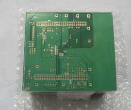
1). 80 *190mm/2up, FR-4 2). 6 layers at 1.4mm thick 3). 35 μm copper weight 4). Green solder mask LPI/White legend 5). ENIG surface finish 6). Blind via from Layer 1 to layer 2 7). Via in pad plugged conductive resin
Industry News | 2003-02-14 08:03:50.0
Provides Devices with Excellent Protection Against EMI and Overcomes Limitations of Metal Cans
Industry Directory | Manufacturer
The exclusive supplier of SIPAD Solid Solder Deposit in North America and the only SIPAD Solid Solder Deposit (SSD) coating service bureau in the world.
Parts & Supplies | Circuit Board Assembly Products
1). 100mm x 98mm/1up, FR-4, 2). 1mm +/-0.1mm,6 Layers 3). 1oz copper finished 3). Green solder mask/white legend 4). Min. hole 0.15mm, 4/4 mil track/gap 5). Blind via layer 1-2, via-in-pad. 6). Immersion gold surface finish
The BEST PCB Epoxy Repair Kit can be used to repair lifted pads and traces as well as build up and repair edge corner damage to PCBs or repair solder mask which has been damaged or removed. By adding colorants a pcb color epoxy kit can be made up cus
With the development of miniaturization of assembly components, the layout area and pattern design area of PCBs have also been continuously reduced, and PCB manufacturers are constantly updating the production process to conform to the development tr
Technical Library | 2019-05-29 01:47:22.0
1.Vias near SMD pads: Solder can flow into the via after melted. As a result cold joint will appear in the end. Check the picture below. 2.Vias on SMD pads: Solder can flow into the via more easier after melted. Check the picture below. 3.Via opening without soldermask covered. When workers solder TH parts by hand, soldering iron can touch vias sometime, then tiny amounts molten solder will stay on vias. This can lead to electrical short easily. We recommend you make all vias tenting (covered by solder mask) if it is possible.
PCBNPI-Professional PCB Fab/PCB Assembly Service Provider From China
Lite Fast SR-1000, a UV Solder Mask, was designed to screen print over conductive traces, landing pads, resistors, fuses and capacitors on Printed Circuit Boards (PCBs) and ceramic substrates. Other applications include metal and various plastics.
Industry News | 2019-11-05 22:22:32.0
1. The definition of Sideplating Sideplating is actually the metalization of the board edge in PCB filed. Edge plating、Border plated、plated contour、side metal, these words can be used too to describe same function. 2. Sideplating Process Drilling - Milling plated Slots - Cleaning - Copper sink 3. Pictures to show the finished board’s sideplating


