
For more information visit: http://www.lpkfusa.com/pls/ The LPKF ProtoLaser S is a fully enclosed laser system for PCB prototyping and production on-demand. It combines advanced laser technology, optics, and x/y table mechanisms that result in high

New Equipment | Assembly Services
Quick turn Prototype PCBs from 24 hour turnaround to high volume printed circuit board production from our domestic plant in USA and/or China facilities. Our Modern 38,000 sq. ft. manufacturing plant with multi-million dollar investment with latest e
Technical Library | 2019-08-14 22:20:55.0
Cleanliness is a product of design, including component density, standoff height and the cleaning equipment’s ability to deliver the cleaning agent to the source of residue. The presence of manufacturing process soil, such as flux residue, incompletely activated flux, incompletely cured solder masks, debris from handling and processing fixtures, and incomplete removal of cleaning fluids can hinder the functional lifetime of the product. Contaminates trapped under a component are more problematic to failure. Advanced test methods are needed to obtain "objective evidence" for removing flux residues under leadless components.Cleaning process performance is a function of cleaning capacity and defined cleanliness. Cleaning performance can be influenced by the PCB design, cleaning material, cleaning machine, reflow conditions and a wide range of process parameters.This research project is designed to study visual flux residues trapped under the bottom termination of leadless components. This paper will research a non-destructive visual method that can be used to study the cleanability of solder pastes, cleaning material effectiveness for the soil, cleaning machine effectiveness and process parameters needed to render a clean part.
Industry News | 2018-10-18 08:32:52.0
How to Prevent Solder Ball and Bridging Defects during the SMT Reflow Process
Career Center | Space Coast, Florida USA | Engineering,Research and Development
Board Level Assembly BGA Expert! We are in need of an Electronic Packaging or Advanced Manufacturing Engineer to work with the Advanced Manufacturing Technology Group of a major Florida based Communications company. Support IR&D and Program activit
Career Center | Melbourne, Florida USA | Engineering
Advanced Manufacturing Technology Position Description Job Description: AMT Engineer � Level 4 Support IR&D and Program activities Division wide working on the development, qualification, and implementation of electronic packaging technologies, wi
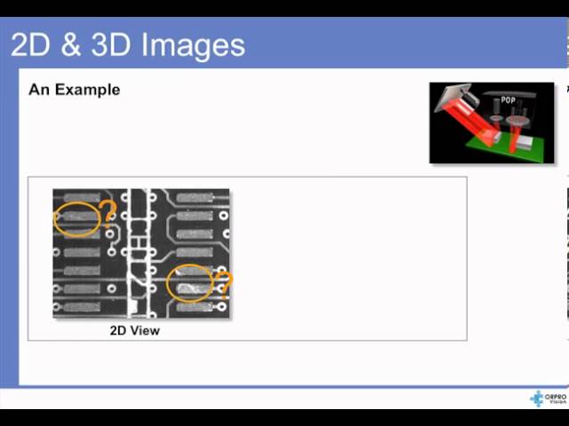
ORPRO Vision SPI Presentation. This presentation introduces the methods and technology used by ORPRO Vision in the Symbion P36 Plus SPI system. For additional information, please contact ORPRO Vision at sales.us@orprovision.com sales.eu@orprovision
Industry Directory | Consultant / Service Provider / Manufacturer
EMS company Laser SMT stencils mfg Tape converting , slitting , die cut Laser modules mfg Distribution materials,components ISO 9001:2015 ISO 13485:2016 AQAP 2110:2016 EN 9120:2018
New Equipment | Fabrication Services
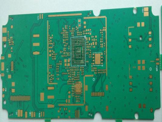
8 Layers Printed Circuit Boards Manufacturing Multilayer PCB Fabrication Product Name: Multilayer PCB Board Material: FR4 Copper thickness 1 oz all layers Board Thickness: 1.6mm Special requirement Impendence Control Fab by Circuit Boar


