Industry News | 2022-01-10 16:55:15.0
The SMTA Capital Chapter Officer team is excited to provide our members with a free technical webinar on "Use of Photonic Soldering to Rework Chip Components" presented by Dr. Vahid Akhavan, Global Application Engineer at NovaCentrix. The presentation will take place on January 20th at 12:00am EST.
Industry News | 2010-07-22 22:37:02.0
IPC — Association Connecting Electronics Industries® has released the B revision of IPC-7351, Generic Requirements for Surface Mount Design and Land Pattern Standard. The leading industry standard for surface mount land pattern design and layout, IPC-7351B provides designers and printed board fabricators with updated guidance on requirements of land pattern geometries used for the surface attachment of electronic components, as well as surface mount design recommendations for achieving the best possible solder joints.
Technical Library | 2007-02-01 10:08:40.0
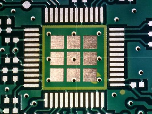
The increased replacement of high lead count SMT devices with BGAs and other high ball count area array packages has brought increased challenges to PCB rework and repair. Often solder mask areas surrounding BGA pad areas are damaged when components are removed.

BEST provides laser machining services for : part marking and demarking, slective solder mask removal, selective coating removal, flex circuit fabrication and precision cable selective stripping. More on using a laser to mark and demark electronic c
New Equipment | Rework & Repair Services
BEST is your source for PCB rework of printed circuit boards. The following services are available to you for performing ECOs on bare printed circuit baords: Pad adds Trace adds Trace cuts Solder mask ablation to rezise pad area Remarking of PCB

PCB pad repair technique demonstrated using the 2-part epoxy method. More on this PCB pad repair technique: http://www.solder.net/services/pcb-repair/pad-and-trace-repair/ More on the recommended epoxy: http://www.soldertools.net/pcb-repair-epoxy-r
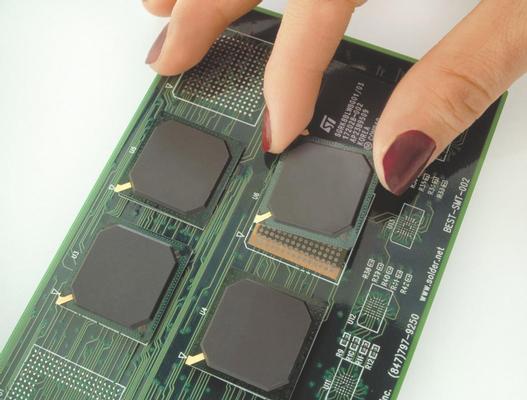
New Equipment | Solder Paste Stencils
Eliminate hours of solder mask damage repair time for bga sites while improving rework yield. Are you frustrated by the time it takes to repair mask damage underneath the BGA during the rework process? Are you squeezed for space on the PCB in an

StencilQuik demonstration video. This breakthrough method allows you to simplify placement/replacement saving 50% or more of time required to rework BGAs or CSPs.This is a well developed BGA rework method. More on the StencilQuik(TM) process here:


.png)

