Technical Library | 2023-01-17 17:22:28.0
The impact of voiding on the solder joint integrity of ball grid arrays (BGAs)/chip scale packages (CSPs) can be a topic of lengthy and energetic discussion. Detailed industry investigations have shown that voids have little effect on solder joint integrity unless they fall into specific location/geometry configurations. These investigations have focused on thermal cycle testing at 0°C-100°C, which is typically used to evaluate commercial electronic products. This paper documents an investigation to determine the impact of voids in BGA and CSP components using thermal cycle testing (-55°C to +125°C) in accordance with the IPC- 9701 specification for tin/lead solder alloys. This temperature range is more typical of military and other high performance product use environments. A proposed BGA void requirement revision for the IPC-JSTD-001 specification will be extracted from the results analysis.
Technical Library | 2019-07-10 23:36:14.0
Pockets of gas, or voids, trapped in the solder interface between discrete power management devices and circuit assemblies are, unfortunately, excellent insulators, or barriers to thermal conductivity. This resistance to heat flow reduces the electrical efficiency of these devices, reducing battery life and expected functional life time of electronic assemblies. There is also a corresponding increase in current density (as the area for current conduction is reduced) that generates additional heat, further leading to performance degradation.
Technical Library | 2020-01-28 00:23:58.0
This paper explores new advances in the reflow soldering process including vacuum technology and warpage mitigation systems. The first topic for discussion will be the implementation of a vacuum process directly in a conventional inline soldering system. The second topic presented is the mitigation of warpage on substrates or wafers.
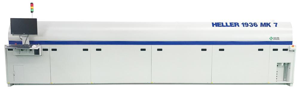
Convection Reflow Oven The World's Best Convection Reflow Oven for High-Throughput The New reflow oven platform revolutionizes the Convection Reflow Oven / Reflow Soldering industry with several new and ground breaking designs! The MK7 convecti
Technical Library | 2023-01-17 17:58:36.0
Heterogeneous integration has become an important performance enabler as high-performance computing (HPC) demands continue to rise. The focus to enable heterogeneous integration scaling is to push interconnect density limit with increased bandwidth and improved power efficiency. Many different advanced packaging architectures have been deployed to increase I/O wire / area density for higher data bandwidth requirements, and to enable more effective die disaggregation. Embedded Multi-die Interconnect Bridge (EMIB) technology is an advanced, cost-effective approach to in-package high density interconnect of heterogeneous chips, providing high density I/O, and controlled electrical interconnect paths between multiple dice in a package. In emerging architectures, it is required to scale down the EMIB die bump pitch in order to further increase the die-to-die (D2D) communication bandwidth. Aa a result, bump pitch scaling poses significant challenges in the plated solder bump reflow process, e.g., bump height / coplanarity control, solder wicking control, and bump void control. It's crucial to ensure a high-quality solder bump reflow process to meet the final product reliability requirements. In this paper, a combined formic acid based fluxless and vacuum assisted reflow process is developed for fine pitch plated solder bumping application. A high-volume production (HVM) ready tool has been developed for this process.
Technical Library | 2023-01-17 17:12:33.0
Reflowed indium metal has for decades been the standard for solder thermal interface materials (solder TIMs or sTIMs) in most high-performance computing (HPC) TIM1 applications. The IEEE Heterogeneous Integration Thermal roadmap states that new thermal interface materials solutions must provide a path to the successful application of increased total-package die areas up to 100cm2. While GPU architectures are relatively isothermal during usage, CPU hotspots in complex heterogeneously-integrated modules will need to be able to handle heat flux hotspots up to 1000W/cm2 within the next two years. Indium and its alloys are used as reflowed solder thermal interface materials in both CPU and GPU "die to lid/heat spreader" (TIM1) applications. Their high bulk thermal conductivity and proven long-term reliability suit them well for extreme thermomechanical stresses. Voiding is the most important failure mode and has been studied by x-ray. The effects of surface pretreatment, pressure during reflow, solder flux type/fluxless processing, and preform design parameters, such as alloy type, are also examined. The paper includes data on both vacuum and pressure (autoclave) reflow of sTIMs, which is becoming necessary to meet upcoming requirements for ultralow voiding in some instances.
Industry News | 2024-02-26 16:22:08.0
HELLER, a leading provider of reflow soldering equipment, concluded its 2024 Sales Kickoff Meeting in Suwon, South Korea on a high note. The meeting brought together sales representatives from all branches and subsidiaries to discuss the company's unified goals and objectives for the year ahead, and to equip them with the tools and knowledge necessary to achieve success.
Industry News | 2003-06-10 08:16:44.0
The following text describes the application of NWA Quality Analyst to quality control in the assembly of electronic components.

New Equipment | Education/Training
Failure Analysis Techniques for Electronics provides an overview of the characterization methods available at ACI Technologies, Inc. for determining the causes of failure in electronics devices. This publication will assist the reader in making inf
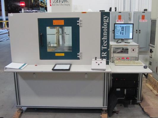
Used SMT Equipment | X-Ray Inspection
CR Technology Model Number: CRX2000 Serial Number: 1S1878.0100 Year 2000-2001 Hamamatsu Tube Type -130kV X-Y-Z indexing table with joystick control 18" x 24" X-Y travel Full 360 degrees rotation and tilt up to 90 degrees BGA / Flip Chip Sold


