Industry News | 2019-01-12 07:42:28.0
IPC – Association Connecting Electronics Industries® announces the winners of the IPC APEX EXPO 2019 Innovation Awards, a celebration of the innovators and forward thinkers who are changing the technological landscape of the electronics industry.
Industry News | 2015-11-25 16:58:05.0
On behalf of the SMTA International Technical Committee, we invite you to submit a 300 word abstract of your research for the 2016 SMTA International 2016 technical conference in Rosemont, Illinois. Papers should describe significant results from experiments, emphasize new techniques, and contain technical, economic or appropriate test data. We are looking for papers on a variety of topics related to electronics manufacturing including advanced packaging/components, assembly, business/supply chain, emerging technologies, harsh environment applications, PCB technology, and process control. Materials must be original, unpublished and non-commercial in nature.
Industry News | 2011-04-20 21:26:17.0
IPC — Association Connecting Electronics Industries® presented Special Recognition, Distinguished Committee Leadership and Committee Service awards and a Presidents Award at IPC APEX EXPO™, held April 10–14, in Las Vegas.
Industry Directory | Manufacturer
Manufacturer of Laser Cut & Chemical Etched Stencils.
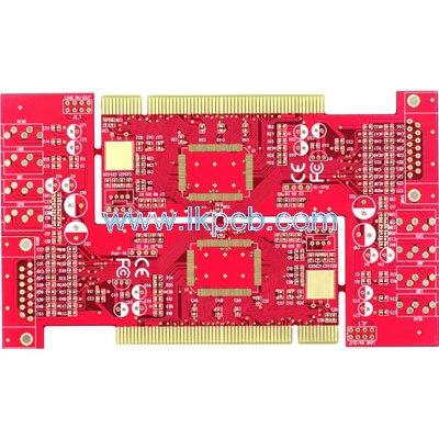
Rogers Material 1.6mm Thickness 2 Layers 1oz copper thickness Gold Plating Surface Treatment red Solder Mask e-test
New Equipment | Fabrication Services
ENIG PCBs with red soldermask Layers: 2 Base material: FR4 Copper thickness: 1oz Board thickness: 1.6mm Min. hole size: 0.45mm Min. line width: 3 mils Min. line spacing: 3 mils Surface finishing: HASL
Technical Library | 2019-09-19 00:28:48.0
The symbiotic relationship between solder masks and selective finishes is not new. The soldermask application is one of the key considerations to ensure a successful application of a selective finish. The selective finish is the final chemical step of the PCB manufacturing process, this is when the panels are at their most valuable and are unfortunately not re-workable. Imperfections are not tolerated, even if they are wholly cosmetic. Quality issues often manifest themselves in the form of a 'ping pong' conversation between the fabricators, the soldermask suppliers and the selective finish suppliers. Without tangible evidence these discussions are difficult to resolve and the selective finish process is usually regarded as responsible. This paper will focus on the chemical characteristics and use them to predict or identify potential issues before they occur rather than specifically name 'critical' soldermasks. It is also the intention of this paper to address the potential of a soldermask to react to common yield hiking practices like UV bumping and oven curing. It is hoped that this awareness will help fabricators to ensure maximum yields by asking the right questions. 'Critical’ soldermasks impact all selective finishes. In this paper, practical experience using immersion tin will be used to highlight the relationship between 'critical' soldermasks and some of the issues seen in the field. The paper will include a novel approach to identify re-deposited volatiles after the reflow.
Industry News | 2019-11-05 22:07:01.0
Tenting a via refers to covering via with soldermask to enclose or skin over the opening. A via is a hole drilled into the PCB that allows multiple layers on the PCB to be connected to each other. A non tented via is just a via that is not covered with the soldermask layer. Leaving these vias exposed or covered has pros and cons depending on the your design and manufacturing requirements.
New Equipment | Solder Paste Stencils
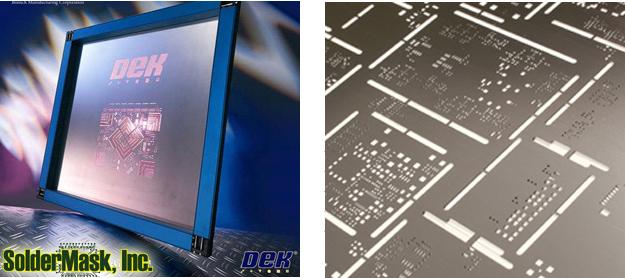
SolderMask Services - Stencils and Custom Stencils Since 1994, SolderMask, Inc. has fabricated solder paste stencil using a photo-chemical etching process. In 1998, we installed our first laser to cut the apertures of the solder paste stencil. Now,


