Industry News | 2019-11-05 22:07:01.0
Tenting a via refers to covering via with soldermask to enclose or skin over the opening. A via is a hole drilled into the PCB that allows multiple layers on the PCB to be connected to each other. A non tented via is just a via that is not covered with the soldermask layer. Leaving these vias exposed or covered has pros and cons depending on the your design and manufacturing requirements.
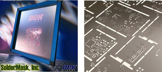
New Equipment | Solder Paste Stencils
SolderMask Services - Stencils and Custom Stencils Since 1994, SolderMask, Inc. has fabricated solder paste stencil using a photo-chemical etching process. In 1998, we installed our first laser to cut the apertures of the solder paste stencil. Now,

Material: Aluminium Layer Coverage: 1Layer Thickness: 1.6mm Surface Technique: HAL Line Width/Space: Solder Mask Color: Black silk screen:white We sincerely hope to establish longtime and friendly business relationship with you. Good quality, re
Industry Directory | Consultant / Service Provider
Quick Turn PCBs, 5 Prototype PCBs at $25.00ea. Fast5Protos delivers quality PCBs in 1-2 days. Free tooling, test, & shipping.
New Equipment | Solder Paste Stencils
Dry Film Solder Application SolderMask, Inc. continues to apply Dry Film Solder Mask (DFSM) on Printed Circuit Boards (PCB) since opening for business in 1985. SolderMask, Inc. works with all DFSM available in the United States. Some of the DFSM ma
Industry News | 2013-11-08 17:12:39.0
ACB is Europe's leading manufacturer of quick-turn and high-reliability prototype and small series PCBs. Typically an early adopter of new and enabling technologies, the company recently took delivery of a top-of-the-range LED-based Direct Imaging (DI) system from Ucamco. Manufactured by Dainippon Screen, Ledia 5 is the PCB industry's fastest DI system, and the only one capable of processing standard soldermask: unique capabilities that, together with ACB's trust in its suppliers, were key to the company's latest investment decision. Working alongside ACB's existing Laser DI system, Ledia 5 handles all ACB's soldermask processing and provides added capacity for dry film exposure. With it, ACB is more flexible and has improved its product quality, yields and capabilities while offering shorter leadtimes for its quick-turn business.
Technical Library | 2011-06-16 18:59:43.0
Based on tests carried out with commercially available chemistry, this paper discusses the advantages available through the use of NEAP processes for inner layer bonding and soldermask pretreatment. The process is characterized with a view to high volume
FR4 2. 0mm, red soldermask, Immersion gold+golden finger


