New Equipment | Test Equipment
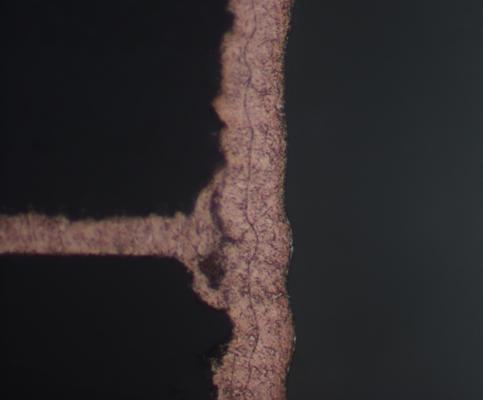
Military-style laboratory services to validate bare boards for product assurance. Testing for delamination, voids, copper thickness, hole quality, proper stack-up, etc. Customer receives all cross-section pucks, boards and laboratory report with reco
1). 6 oz (210μm) on BOT side. 2). 139.99*110.85mm=1 pcb 3). Base material: FR-4 4). 4 Layer, 1.6mm thick 5). Green solder mask/ white legend 6). Immersion gold. 7). Stack-up ---------- OVERLAY (TOP) ---------- SOLDER MASK (TOP)
Industry News | 2018-10-18 10:43:28.0
Suggested 14 and 16 Layer Board Layouts
Industry News | 2018-10-18 11:01:38.0
What Design Files Are Necessary for PCB Manufacturing & Assembly?
Technical Library | 2008-02-26 15:02:19.0
More and more chip packages need multi-GHz RF structures to meet their performance targets. The ideal chip package needs to combine RF features with Digital features for these applications. They drive low-loss, controlled impedance transmission lines, flexibility in assigned signal and power layers, and clearances of various shapes in power layers. Building these features in a chip package is difficult without making the stack-up very thick or compromising the reliability of the product. In the present paper, we have designed and built a flip-chip package test vehicle (TV) to make new RF structures, using Z-axis interconnection (Zinterconnect) building blocks.
Technical Library | 2017-06-15 00:44:19.0
Ceramics packages are being used in the electronics industry to operate the devices in harsh environments. In this paper we report a study on acoustic imaging technology for nondestructively inspecting underfill layers connecting organic interposers sandwiched between two ceramics substrates.First, we inspected the samples with transmission mode of scanning acoustic tomography (SAT) system, an inspection routine usually employed in assembly lines because of its simpler interpretation criteria: flawed region blocks the acoustic wave and appears darker. In this multilayer sample, this approach does not offer the crucial information at which layer of underfill has flaws. To resolve this issue, we use C-Mode Scanning in reflection mode to image layer by layer utilizing ultrasound frequencies from 15MHz to 120MHz. Although the sample is thick and contains at least 5 internal material interfaces, we are able to identify defective underfill layer interfaces.
Manufacture and Characterization of a Novel Flip-Chip Package Z-interconnect Stack-up with RF Structures Manufacture and Characterization of a Novel Flip-Chip Package Z-interconnect Stack-up with RF Structures More and more chip packages need
SMTnet Express, December 9, 2021, Subscribers: 26,314, Companies: 11,473, Users: 26,968 Reliability of Stacked Microvia Reliability of Microvia has been a concern since microvias were introduced to our industry. This study
| https://pcbasupplies.com/hang-stack-bins-1/
Hang & Stack Bins Archives - PCBASupplies Login Create Account Contact View My Cart Menu × Categories Hand Soldering & Rework Automation Tooling PCB Support Systems Soldering Robots Material Handling Dry Storage Cabinets Component Handling Selective Solder Nozzles Pick
KingFei SMT Tech | http://www.smtspare-parts.com/sale-9469374-thickness-sensor-n510015037aa-smt-spare-parts-cm212-photo-sensor-smt-parts.html
Thickness Sensor N510015037AA SMT Spare Parts CM212 Photo Sensor SMT Parts Leave a Message We will call you back soon! Your message must be between 20-3,000 characters


