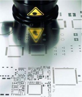
SMT stencils for standard and ultra-fine pitch applications
New Equipment | Solder Paste Stencils
We use fine grain stainless steel for the base of all our Stencils, All Stencils are cut on LPKF lasers which ensures the best quality for optimum paste release. Our Stencils are offered in thicknesses from .0015" to .0020". Our laser cut Stencils c
Training Courses | | | PCB Assembly Courses
The PCB assembly courses provide knowledge of different processes and equipment used in TH and SMT assembly of printed circuit boards.
Technical Library | 2010-03-25 06:26:37.0
The complexity of Printed Circuit Assembly process is increasing day by day and causing productivity issues in the industry, introducing ultra fine pitch components (pitch less than 15mil) in PCA is a challenge to minimize risk of defects as solder short, dry solder. This paper is focusing on minimizing these defects.

http://www.ddmnovastar.com/stencil-printers - DDM Novastar Stencil Printers are designed for short to medium run PCB assembly. Ranging from manual to semi-automatic, these durable, easy-to-use systems provide repeatable, reliable results. Greatly r
New Equipment | Solder Paste Stencils
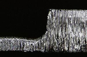
Through the increase of mixed technologies, stepped stencils have gained importance to the electronic assembly manufacturer. If the solder paste quantity can no longer be adequately regulated by adjusting Step/Relief Stencil Picture the pad sizes, st
Industry Directory | Consultant / Service Provider
PCB assembly services, both US and offshore. We handle basic through-hole to standard surface mount to ultra-fine pitch. Quote and order PCB fabrication and assembly online.
New Equipment | Solder Paste Stencils
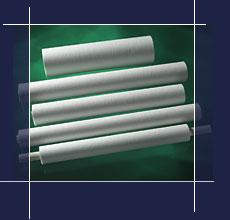
EasyBraid’s stencil rolls are designed for use in SMT screen printing lines which keep stencil apertures clear of paste residues during the automatic screen printing process. They also clean the bottom of stencils, keeping them free from paste and fl
Quality stencils for coarse and fine pitch solder and epoxy deposition. Cost and quality competitive against laser cut stencils. Twenty-four turn, no premium!
Technical Library | 2015-08-25 13:51:27.0
The stencil printing process is one of the most critical processes in the electronic production. Due to the requirement: "faster and smaller" it is necessary to place components with different paste volume close together without regard to solder paste printing. In our days it is no longer possible to control the solder paste volume only by adjustment of the aperture dimensions. The requirements of solder paste volumes for specific components are realized by different thicknesses of metal sheets in one stencil with so called step stencils. The step-down stencil is required when it is desirable to print fine-pitch devices using a thinner stencil foil, but print other devices using a thicker stencil foil. The paper presents the innovative technology of step-up and step-down stencils in a laser cutting and laser welding process. The step-up/step-down stencil is a special development for the adjustment of solder paste quantity, fulfilling the needs of placement and soldering. This includes the laser cutting and laser welding process as well as the resulting stencil characteristics and the potential of the printing process.


