Industry News | 2018-12-08 03:35:10.0
Top 10 Consumer Electronics Companies in the World
Industry News | 2018-12-08 03:22:25.0
Electronic Components, Parts and Their Function
Industry News | 2014-01-17 12:52:25.0
BEST Inc., has developed a line of Kapton™ SMT stencils for the prototype assembly market. These stencils, available in 4,5 and 6 thicknesses, present very flat coplanar printing surfaces for solder paste printing. . They are designed to be used when the there are very few boards to be made at one time and the pitch of the components is 1.00 and above.
Industry News | 2016-10-25 09:47:33.0
Learn about SMT assembly from SME Phil Zarrow in Chicago
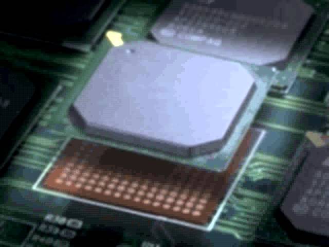
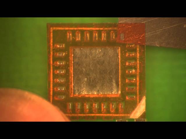
This video describes the BEST BGA rework and BGA rework services capabilities. What is described in this movie are the people, processes and tools unique to BEST and how that impacts its customers. The advanced equipment set including multiple refl
Industry News | 2018-11-06 20:35:12.0
Kurtz Ersa today announced that Krypton Solutions LLC has invested in several new systems from Ersa for its new facility. A long-time Ersa customer with equipment at its Plano, TX facility, Krypton selected Ersa to help furnish its new facility in San Jose, CA.
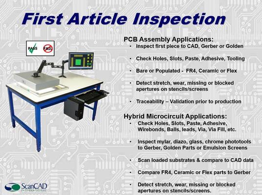
Inspection and Data Creation Tool for the Stencil / Screen Fabrication Industry. World's leading solder paste stencil & emulsion screen inspection system. Used by both stencil/screen fabricators and users to detect errors BEFORE production, elimina
Industry News | 2014-06-17 21:50:29.0
SMT International has just introduced AMTECH VS-213 (a.k.a. the VOIDSTOPPER), a no-clean, lead-free solder paste formula that is 100% halogen-free based on all testing methods, including Oxygen Bomb Combustion and Ion Chromatography.


winsouce.jpg)