Industry News | 2017-03-01 15:05:28.0
IPC presented Committee Leadership, Distinguished Committee Service and Special Recognition Awards at IPC APEX EXPO® at the San Diego Convention Center. The awards were presented to individuals who made significant contributions to IPC and the industry by lending their time and expertise through IPC committee service.

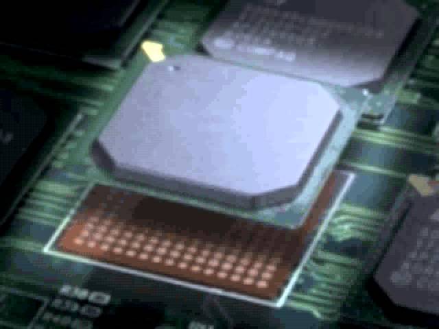
Teaching video on PCB through hole repair. BEST instructors teach the method for repair of a damaged eyelet using a multitude of different close up and angled views. Repair is completed per the IPC 7721 instructions. http://www.solder.net
Industry News | 2021-04-22 17:08:17.0
New Advanced Thermal Solutions' Devices can Continuously Store Biological Materials at Temperatures as Low as -123°F
Technical Library | 2020-07-15 18:49:03.0
Via Filling • Through Hole Vias - IPC-4761 – Plugging – Filling – Filled & Capped • MicroviaFilling and Stacked Vias
Technical Library | 2017-08-10 01:23:22.0
This paper demonstrates the high frequency performance and thermo-mechanical reliability of through vias with 25 μm diameter at 50 μm pitch in 100 μm thin glass substrates. Scaling of through via interconnect diameter and pitch has several electrical performance advantages for high bandwidth 2.5D interposers as well as mm-wave components for 5G modules.
Technical Library | 2019-07-17 17:56:34.0
The increased demand for electronic devices in recent years has led to an extensive research in the field to meet the requirements of the industry. Electrolytic copper has been an important technology in the fabrication of PCBs and semiconductors. Aqueous sulfuric acid baths are explored for filling or building up with copper structures like blind micro vias (BMV), trenches, through holes (TH), and pillar bumps. As circuit miniaturization continues, developing a process that simultaneously fills vias and plates TH with various sizes and aspect ratios, while minimizing the surface copper thickness is critical. Filling BMV and plating TH at the same time, presents great difficulties for the PCB manufactures. The conventional copper plating processes that provide good via fill and leveling of the deposit tend to worsen the throwing power (TP) of the electroplating bath. TP is defined as the ratio of the deposit copper thickness in the center of the through hole to its thickness at the surface. In this paper an optimization of recently developed innovative, one step acid copper plating technology for filling vias with a minimal surface thickness and plating through holes is presented.
Technical Library | 2012-02-02 19:09:53.0
A miniaturized wafer-level packaged MEMS acceleration switch with through silicon vias (TSVs) was fabricated, based on technologies suitable for harsh environment applications. The high aspect ratio TSVs were fabricated through the silicon-on-insulator (S
The Foundation for Scientific and Industrial Research - SINTEF
Technical Library | 2020-07-22 19:39:05.0
The PWB industry needs to complete reliability testing in order to define the minimum copper wrap plating thickness requirement for confirming the reliability of PTH structures. Predicting reliability must ensure that the failure mechanism is demonstrated as a wear-out failure mode because a plating wrap failure is unpredictable. The purpose of this study was to quantify the effects of various copper wrap plating thicknesses through IST testing followed by micro sectioning to determine the failure mechanism and identify the minimum copper wrap thickness required for a reliable PWB. Minimum copper wrap plating thickness has become an even a bigger concern since designers started designing HDI products with buried vias, microvias and through filled vias all in one design. PWBs go through multiple plating cycles requiring planarization after each plating cycle to keep the surface copper to a manageable thickness for etching. The companies started a project to study the relationship between Copper wrap plating thickness and via reliability. The project had two phases. This paper will present findings from both Phase 1 and Phase 2.


