Advance Devices, Inc. offers Smart Tweezers LCR Meter - excellent tool for identification testing of SMD Components.
Industry Directory | Consultant / Service Provider / Manufacturer
Delkin Devices, Inc. is an independently owned business and the largest US memory card manufacturer in San Diego, CA.
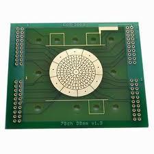
General specification for Microwave/RF PCB Layer count: 1-6 Board thickness: 0.2-3.2mm Copper thickness: 0.5-4oz Dielectric Constant(DK): 2.2-10.3 Min trace width/spacing: 4/4mil Min drill hole size: 0.2mm Surface treatment: HAL(Lead free), I
SemiPack's fully automated tinning services restore the finish and soldering properties of leads for both through-hole and surface mount devices. SemiPack provides both RoHS-SnPb and SnPb-RoHS conversions. Tinned components are processed in com
Electronics Forum | Tue Oct 22 15:32:09 EDT 2002 | ruppertg125
We are a military contractor and need to build to IPC610 class3. We are receiving many parts with palladium leads and currently use a No-clean solder paste. We have evaluated OA pastes with very little improvements. Without a touch up of all leads th
Electronics Forum | Tue Sep 09 20:32:10 EDT 2003 | davef
The maximum ratio of gold weight to solder alloy weight can be calculated, to help prevent a problem from excessive gold-tin intermetallic compound (i.e., AuSn4). For the equation and its derivation, please refer to "The Use of Capillary Action Measu
Industry News | 2010-12-03 21:35:04.0
Eastern Europe's growing electronics assembly industry faces new challenges, especially with the adoption of lead-free technology. To connect manufacturers with solutions to these challenges, IPC — Association Connecting Electronics Industries® is holding the IPC Conference on Quality, Reliability and Acceptability for Electronics Manufacturing in Budapest, Hungary, on 22–24 February 2011.
Industry News | 2011-10-21 13:55:23.0
IPC’s Solder Products Value Council (SPVC) is actively urging tin smelters to become smelters of conflict-free minerals and recommends the Electronic Industry Citizenship Coalition/Global e-Sustainability Initiative (EICC/GESI) Conflict-Free Smelter (CFS) program.
Parts & Supplies | Circuit Board Assembly Products
PULANG TECHNOLOGY CO,.LTDOffers electronic manufacturing services including PCB designing, electronic contract manufacturing including electronic product design, electronic product development, electronic product repair, PCB manufacturing, electronic
Technical Library | 2019-10-21 09:58:50.0
An ACI Technologies customer inquired regarding printed circuit board(PCB) failures that were becoming increasingly prevalent after the SMT (surface mount technology) manufacturing process. The failures were detected by electrical testing, but were undetermined as to the location and specific devices causing the failures. The failures were suspected to be caused predominately in the BGA (ball grid array) devices located on specific sites on this 16 layer construction. Information that was provided on the nature of the failures (i.e., opens or shorts) included high resistance shorts that were occurring in those specified areas. The surface finish was a eutectic HASL (hot air solder leveling) and the solder paste used was a water soluble Sn/Pb(tin/lead).
Technical Library | 2019-05-23 10:30:22.0
Increasing I/O numbers, device complexity, and product miniaturization requires high precision bonding tools, and sophisticated equipment. Careful consideration should be given to wedge geometry while selecting the tool for a fine pitch wire bonding application. Wire bonding is a process that creates an electrical connection between a die and a substrate or lead typically using gold or aluminum wire. Wedge bonding is a specific type of wire bonding that uses a wedge shaped tool to create the welds. The design of the wedge tool has changed very little over the past decade. The wire is fed at an angle through the back of the wedge. This angle is typically 30 to 60 degrees and is application dependent. Some applications require a higher feed angle due to package clearance issues. Some deep access applications require a 90 degree feed angle. In this configuration, the wire is fed through a hole in the shank of the wedge tool. Wire feed is shown in Figure 1.

ACI Technologies Inc. (ACI) is a scientific research corporation dedicated to the advancement of electronics manufacturing processes and materials for The Department of Defense and industry. This video provides an overview of our commercial service

1200MM/1500MM Online SPI , Big Size Solder Paste Inspection Machine mail: sales@smtlinemachine.com whatapp/wechat:+8613537875415 Specification: 技术参数/Parameters 技术平台/Technology Platform super big size platform 适用
Training Courses | | | PCB Rework and Hand Soldering Courses
The PCB rework and hand soldering courses courses cover techniques of rework and repair of PCBs, BGAs and other electronics assemblies, and teach fundamentals of soldering of electronics assemblies.
Events Calendar | Wed Apr 20 00:00:00 EDT 2022 - Wed Apr 20 00:00:00 EDT 2022 | ,
Virtual Course: Selection Criteria of Surface Finish for Next Generation PCB Technologies
Events Calendar | Mon Apr 23 00:00:00 EDT 2018 - Thu Apr 26 00:00:00 EDT 2018 | Shanghai, China
SMTA China East Conference 2018
Career Center | Shen Zhen, China | Management,Sales/Marketing
Working in GLORYPCB for 10 years.knowing electronic supply chain very well. especially for PCB PCBA assembly and other Electronic Manufacturing Service.Glorypcb is a professional electronic manufacturer located in Shenzhen with three facilities.offe
Career Center | Houston, Texas USA | Engineering,Management,Quality Control,Technical Support
Seasoned Process & Quality Engineer. Degreed Chemical Engineer. 20+ years in Electronics Semiconductor manufacturing. Proficient in Quality Statistical tools, Design of Experiments, FMEAs, APQP, PPAP, ISO 9000, ISO/TS 16949 etc.
SMTnet Express, August 7, 2014, Subscribers: 23058, Members: Companies: 13975, Users: 36604 Gold Embrittlement In Lead-Free Solder. Craig Hillman, Nathan Blattau, Joelle Arnold, Thomas Johnston, Stephanie Gulbrandsen; DfR Solutions , Julie Silk
Horizontal Convection Reflow Technology Defined Horizontal Convection Reflow Technology Defined Leading up to the development of lead-free soldering alloys, Horizontal Convection* was developed for the reflow process. Getting the correct
ASYMTEK Products | Nordson Electronics Solutions | https://www.nordson.com/en/divisions/sonoscan/support/application-notes/1058-lead-delaminations
. Tinning is sometimes done with a noble metal such as gold to improve the adhesion of bond wires. The problem is that some molding compounds do not adhere well to the noble metals
Imagineering, Inc. | https://www.pcbnet.com/blog/pcb-prototyping-what-you-should-be-looking-for/
. Copper weights range from 1 to 4g. Finish plating can be leaded solder, or any following RoHS-compliant finishes: lead-free solder, immersion gold, immersion silver, white tin, or OSP


