Industry Directory | Consultant / Service Provider
CCN provides impedance, loss, and s-parameter test systems for PCB production testing and design. We also provide test services to support products or customers needing traceable dielectric constant and transmission line testing.
Industry Directory | Manufacturer
Pelco is a world leader in the design, development and manufacture of video and security systems and equipment ideal for any industry
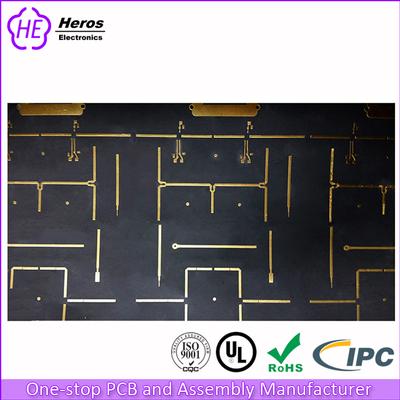
Layer Count: 2L Board Thickness: 0.8mm Dimension: 140*85mm Material: Rogers RO5880 Surface Copper: 35μm Min Hole Diameter: 2.0mm Min line Width/Space: N/A Surface Finish: ENIG Do you need a PCB for special signal requirement into your products? High
New Equipment | Test Equipment
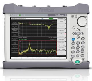
Cable & Antenna Analyzer To keep up in today s rapidly evolving wireless communications market, you need tools that enable you to efficiently maintain legacy networks in addition to the new 3G and 4G networks now being installed. And as the market
Electronics Forum | Wed Apr 30 08:00:33 EDT 2003 | pjc
Jason, In Transmission AXI the entire solder joint volume is imaged, not just a slice (no missing information) as with Cross-Section. Also, there is no signal loss from mechanical or digital image reconstruction (highest contrast and edge strength).
Electronics Forum | Thu Jan 07 14:21:43 EST 2021 | nicole09pay
I'm new to SMT circuit design and I'm wondering is that okay to connect a SMD component to a transmission line (microstrip) which has a width larger than that of the component? My simulation results show that its fine but I'm not sure if it causes si
Used SMT Equipment | Pick and Place/Feeders
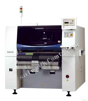
Device Name: Samsung SM411, Samsung SM411 Mater, Second-hand Samsung SM411 Mater Equipment Profile: The SM411 uses the Samsung Patent On The Fly identification method and the double cantilever structure to achieve the chip component 42,000 CPH and
Used SMT Equipment | General Purpose Test & Measurement
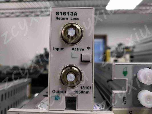
Key Features & Specifications Return loss dynamic range > 75 dB Return loss uncertainty down to ±0.25 dB with external broadband source Wide operating wavelength range: 1250 nm to 1640 nm Built-in Power Monitor and Laser Source: 131
Industry News | 2019-06-16 19:33:20.0
Super PCB is pleased to announce that the company offers high density interconnect (HDI) PCBs. HDI products have a higher wiring density per unit area than traditional PCBs and offer faster transmission, less signal loss, fewer delays and are more compact.
Technical Library | 2015-04-30 20:17:03.0
Higher-speed signal transmission is increasingly required on a printed circuit board to handle massive data in electronic systems. So, signal transmission loss of copper wiring on a printed circuit board has been studied. First, total signal loss was divided into dielectric loss and conductor loss quantitatively based on electromagnetic theory. In particular, the scattering loss due to surface roughness of copper foil has been examined in detail. And the usefulness of the copper foil with low surface roughness has been demonstrated.
Technical Library | 2019-02-13 13:45:11.0
Development of information and telecommunications network is outstanding in recent years, and it is required for the related equipment such as communication base stations, servers and routers, to process huge amount of data in no time. As an electrical signal becomes faster and faster, how to prevent signal delay by transmission loss is a big issue for Printed Circuit Boards (PCB) loaded on such equipments. There are two main factors as the cause of transmission loss; dielectric loss and conductor loss. To decrease the dielectric loss, materials having low dielectric constant and low loss tangent have been developed. On the other hand, reducing the surface roughness of the copper foil itself to be used or minimizing the surface roughness by modifying surface treatment process of the conductor patterns before lamination is considered to be effective in order to decrease the conductor loss. However, there is a possibility that reduction in the surface roughness of the conductor patterns will lead to the decrease in adhesion of conductor patterns to dielectric resin and result in the deterioration of reliability of PCB itself. In this paper, we will show the evaluation results of adhesion performance and electrical properties using certain type of dielectric material for high frequency PCB, several types of copper foil and several surface treatment processes of the conductor patterns. Moreover, we will indicate a technique from the aspect of surface treatment process in order to ensure reliability and, at the same time, to prevent signal delay at the signal frequency over 20 GHz.
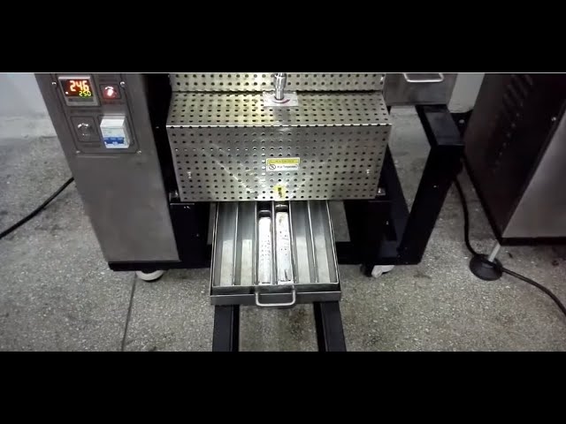
BESTEMP reflow checker 6 channel temperature profiler Reflow soldering temperature tester Characteristic: 1..High efficiency, data can be stored up to 16 times continuously, and can be downloard to computer for group data viewing. 2. Modular analys
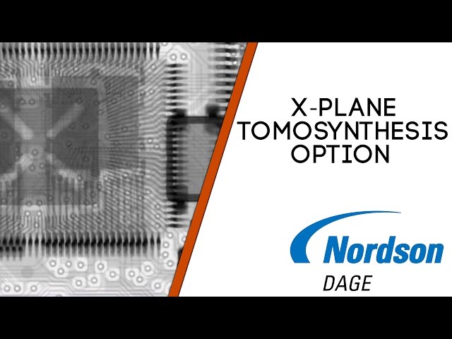
The X-Plane™ option uses a proprietary, patent applied for, tomosynthesis (or CT) technique to create 2-D X-ray slices in any plane of a printed circuit board assembly without the need to cut or destroy the board. In this way, the superior image qual
Training Courses | ONLINE | | PCB Design Courses
The PCB design courses teach students the process, techniques and tools needed to design layout of printed circuit boards.
Events Calendar | Wed Apr 20 00:00:00 EDT 2022 - Wed Apr 20 00:00:00 EDT 2022 | ,
Virtual Course: Selection Criteria of Surface Finish for Next Generation PCB Technologies
Events Calendar | Wed Apr 19 00:00:00 EDT 2017 - Fri Apr 21 00:00:00 EDT 2017 | Nara, Japan
Ceramic Interconnect and Ceramic Microsystems Technologies (CICMT 2017)
International Microelectronics Assembly and Packaging Society (IMAPS)
Career Center | San Jose, CA, California USA | Engineering,Production,Research and Development
Senior PCB Designer: Want to be part of an exciting pre-IPO enterprise B2B company working on the cutting edge of internet-of-things, artificial intelligence & agents, blockchain, and manufacturing technology? This well-funded venture-backed co
SMTnet Express, April 30, 2015, Subscribers: 22,686, Members: Companies: 14,334 , Users: 38,119 Signal Transmission Loss due to Copper Surface Roughness in High-Frequency Region Elaine Liew; Mitsui Copper Foil Malaysia, Shah Alam Malaysia, Taka
SMTnet Express, February 13, 2014, Subscribers: 26508, Members: Companies: 13577, Users: 35737 Why Signal Always Be Loss in a High Speed, High Frequency Transmission Line. by Albert Chen; Elite Material Co., Ltd. The high speed transmission
Imagineering, Inc. | https://www.pcbnet.com/capabilities/fabrication/hdi/
) for a higher wiring density per unit area. They’re ideal for using smaller, future-driven components on a wide scale. They offer faster signal transmission and a significant reduction in signal loss and crossing delays
| http://etasmt.com/cc?ID=te_news_media,10561&url=_print
. Look at the heating length. The same price, the longer the heating section, the higher the cost performance. 3. Transmission and transportation Better reflow soldering is in operation
winsouce.jpg)
.gif)


