New Equipment | Test Equipment
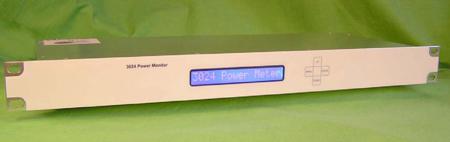
The COMM-connect 3024 RF Power Monitor can control up to 8 external RF Measuring heads. The high dynamic range with external couplers and RF measuring heads cover from 1W to 1MW. The Power conversion algorithms handles multi carrier, multi mode, peak
Used SMT Equipment | In-Circuit Testers
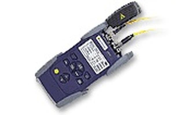
JDSU OLT55-2286/01 OLT-55 Optical Loss Test Set, integrated Laser source: wavelength 1310 and 1550 nm, power range -7 to 0 dBm, Fiber style 9/125 m SM, integrated Power meter: wavelength range 780 to 1650nm, power range -70 to +20 dBm, Ge photodi

Used SMT Equipment | In-Circuit Testers
JDSU OLT55-2286/02 OLT-55 Optical Loss Test Set, integrated Laser source: wavelength 1310 and 1550 nm, power range -7 to 0 dBm, Fiber style 9/125 m SM, integrated Power meter: wavelength range 780 to 1650nm, power range -70 to +20 dBm, Ge photodi

Used SMT Equipment | In-Circuit Testers
JDSU OLT55-2286/02 OLT-55 Optical Loss Test Set, integrated Laser source: wavelength 1310 and 1550 nm, power range -7 to 0 dBm, Fiber style 9/125 m SM, integrated Power meter: wavelength range 780 to 1650nm, power range -70 to +20 dBm, Ge photodi

Used SMT Equipment | In-Circuit Testers
JDSU OLT55-2286/01 Details JDSU OLT55-2286/01 OLT-55 Optical Loss Test Set, integrated Laser source: wavelength 1310 and 1550 nm, power range -7 to 0 dBm, Fiber style 9/125 m SM, integrated Power meter: wavelength range 780 to 1650nm, power ra
New Equipment | Cleaning Equipment
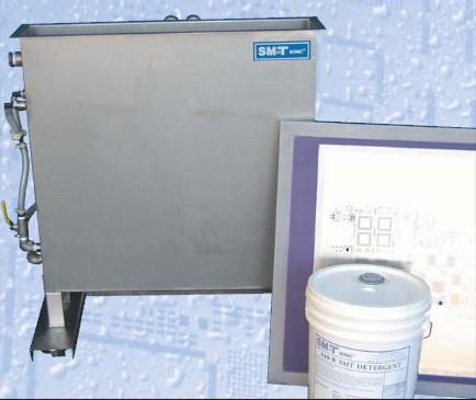
The Low Cost / High Efficiency Stencil Cleaner Stainless Steel Construction Cleans Stencils up to 29" x 29" Low profile allows easy loading and unloading Side mounted “sweep frequency” ultrasonic transducers with 10 year limited warr
Industry News | 2017-05-22 17:36:43.0
KYZEN is pleased to announce that Mike Bixenman, DBA will present at the International Conference on Soldering & Reliability (ICSR) held in conjunction with the Toronto SMTA Expo & Tech Forum. Bixenman will present the paper entitled, “Reliable Microelectronic Assembly Process Design Test Methods – A Non-Standard Approach” at 2:30 p.m. on Wednesday, June 7, 2017 at the Edward Village Markham in Ontario.


Rugged Material Feeding Unit for Highly Abrasive Dispensing Media With High Viscosity. Loading of Material From 20-Litre Drums With the Patented Scheugenpflug Barrel Follower Plate. The barrel (hobbock, pail) is positioned on the ergonomic hobbock d
Technical Library | 2015-07-16 17:24:23.0
Qualification of electronic hardware from a corrosion resistance standpoint has traditionally relied on stressing the hardware in a variety of environments. Before the development of tests based on mixed flowing gas (MFG), hardware was typically exposed to temperature-humidity cycling. In the pre-1980s era, component feature sizes were relatively large. Corrosion, while it did occur, did not in general degrade reliability. There were rare instances of the data center environments releasing corrosive gases and corroding hardware. One that got a lot of publicity was the corrosion by sulfur-bearing gases given off by data center carpeting. More often, corrosion was due to corrosive flux residues left on as-manufactured printed circuit boards (PCBs) that led to ion migration induced electrical shorting. Ion migration induced failures also occurred inside the PCBs due to poor laminate quality and moisture trapped in the laminate layers.


